
Method for analyzing manufacturing data

a manufacturing data and data analysis technology, applied in the field of manufacturing data analysis, can solve the problems of difficult isolating any one out-of-spec source, no two chips are identical, and modern semiconductor manufacturing processes are very complex, and achieve the effect of increasing the amount of data availabl

Inactive Publication Date: 2007-02-06
BELL SEMICON LLC
View PDF6 Cites 7 Cited by
  • Summary
  • Abstract
  • Description
  • Claims
  • Application Information

AI Technical Summary

Benefits of technology

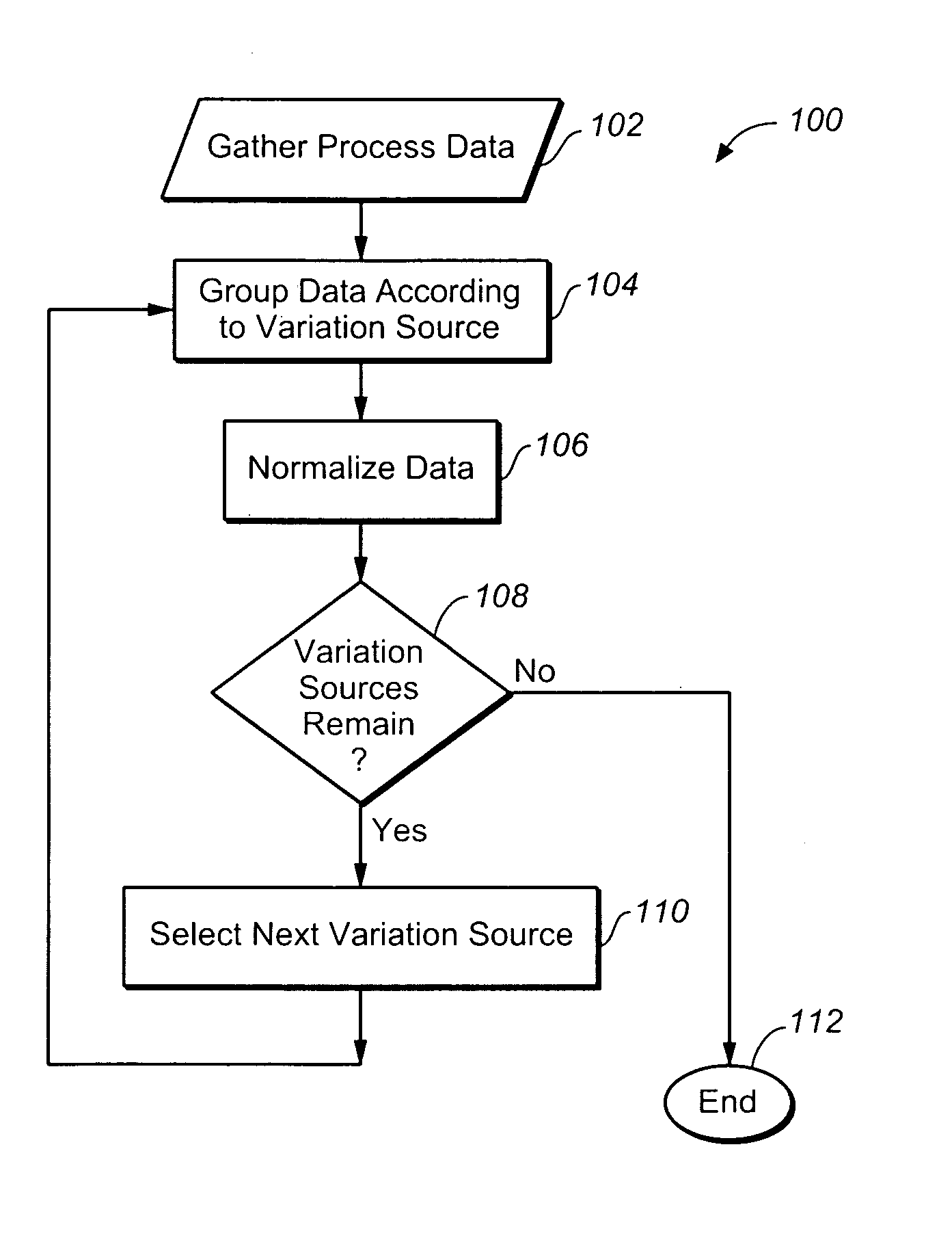
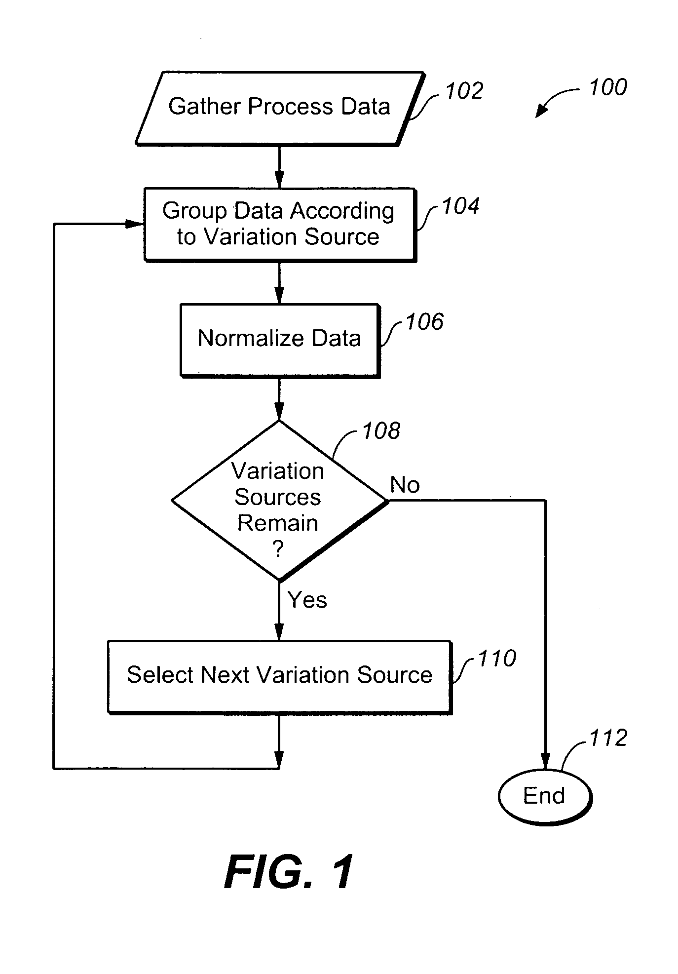
[0014]The present invention is a method of manufacturing, e.g., integrated circuits, and of managing the manufacturing process. Product unit (circuit) variation data is collected from clustered product units (wafer sites). Collected data is grouped according to a selected manufacturing parameter. Each group is normalized for the selected manufacturing parameter. Normalized groups are combined. Normalized process data is checked for variances and the data is regrouped and renormalized until variances are no longer found. Each identified variance is correlated with a likely source. Then, each said likely source is addressed, e.g., a tool is adjusted or replaced, to minimize variances. Thus, by rendering data collected from semiconductor die that are processed on wafers grouped into lots, the method of the present invention provides more informative analysis results from new lot level statistical variables.

Problems solved by technology

However, realistically, no two chips are identical.
Modern semiconductor manufacturing processes are very complex, perhaps, including hundreds of individual process steps from selecting a blank wafer, to forming the layers, to producing the final working product.
In addition with multiple tools used at each process step, each tool adding some parametric variation, it is no surprise that the combined influence of all of these independent variations on different parameters makes isolating any one out-of-spec source difficult.
Very often, prior art approaches identified numerous false positive and false negatives.
Additionally, even if the product is “in-spec,” currently, the only way to assure that it remains in-spec may be to limit process parameter variation, thereby limiting drift towards process window edges, where performance may degrade.
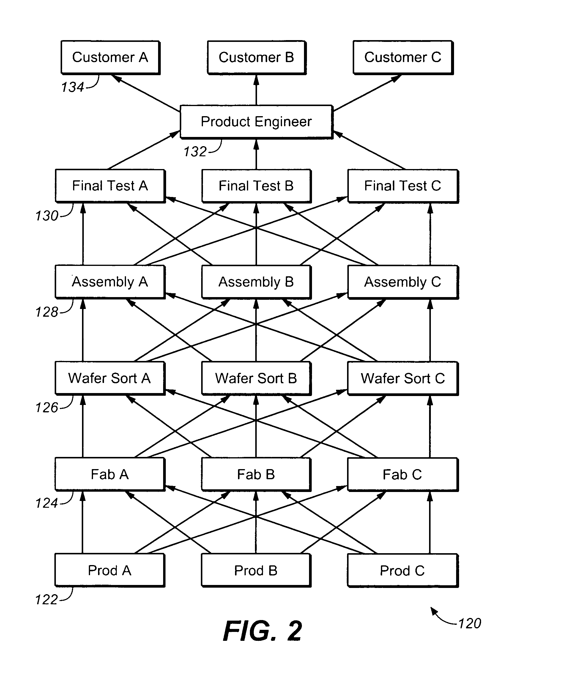
The challenge for the PE is to identify variances from natural groupings of the process flow data that may be arising from different sources, i.e., different test facilities, different tools used at the same step, etc.
However, the data points are seldom independent of each other.
First, since there are so many process steps and because the targeted parameter differences may be so small, a huge amount of data may be necessary to statistically correlate the results.
Second, lots and wafers within each lot are not randomly processed.
Otherwise, making such an assumption would result in a false difference from the statistical comparison of the lot data among the three tools at step 2 where in actuality none exists.
This restriction greatly reduces the amount of available data, exacerbating the need for large amounts of data for analysis.

Method used


Image

  • Method for analyzing manufacturing data
  • Method for analyzing manufacturing data
  • Method for analyzing manufacturing data

Examples


Embodiment Construction

[0030]The reduction in the amount of available data for correlating process parameter variations with individual sources of the process parameter variations described above may be avoided by a way to correlate process parameter variations to individual sources of those variations using the entire population of characterization data as follows.

[0031]Turning now to the drawings and more particularly, FIG. 1 shows a method 100 of selectively removing a source of product variation so that an entire collection of process data may be used to identify additional sources of process variation. Each process step may affect the mean value of a parameter or increase the variance of the parameter. For any manufacturing process wherein each process step contributes to product variations additively, the preferred embodiment method 100 selectively removes variation sources for enhanced analysis. Although described hereinbelow with reference to integrated circuits and semiconductor manufacturing, th...


PUM


Abstract

A method of manufacturing, e.g., integrated circuits, and of managing a manufacturing process. Product unit (circuit) variation data is collected from clustered product units (wafer sites). Collected data is grouped according to a selected manufacturing parameter. Each group is normalized for the selected manufacturing parameter. Normalized groups are combined. Normalized process data is checked for variances and the data is regrouped and renormalized until variances are no longer found. Each identified variance is correlated with a likely source. Then, each said likely source is addressed, e.g., a tool is adjusted or replaced, to minimize variances.

Description

BACKGROUND OF THE INVENTION[0001]1. Field of the Invention[0002]The present invention is related to manufacturing data analysis and more particularly to semiconductor process manufacturing data analysis.[0003]2. Background Description[0004]Typically, integrated circuit chips are manufactured by forming a grid of chips clustered onto a single semiconductor wafer, e.g., a silicon wafer. The grid may have a thousand or more chip (die) sites or locations. Chip patterns may be formed on the wafer photolithographically, layer by layer. Once all of the layers have been formed the wafer, it is diced to separate the individual chips (die). Furthermore, groups of 20 or more wafers are normally formed more or less at the same time. Each of these groups is called a lot. Ideally, every chip on each wafer in every lot forms identically with every other chip on every other wafer in every other lot, such that all chips of the same chip type are identical. However, realistically, no two chips are id...

Claims


Application Information

Patent Timeline
Patent Type & Authority Patents(United States)
IPC IPC(8): G06F17/10G05B13/02
CPCG06Q10/043
Inventor ABERCROMBIE, DAVID
Owner BELL SEMICON LLC
Learn More