

Multiple data rate memory interface architecture
a memory interface and data rate technology, applied in the direction of logic circuit coupling/interface arrangement, pulse technique, instruments, etc., can solve the problems of limited clock signal speed, stringent timing requirements,/o architectures
- Summary
- Abstract
- Description
- Claims
- Application Information
AI Technical Summary
Benefits of technology
Problems solved by technology
Method used
Image



Examples
Embodiment Construction
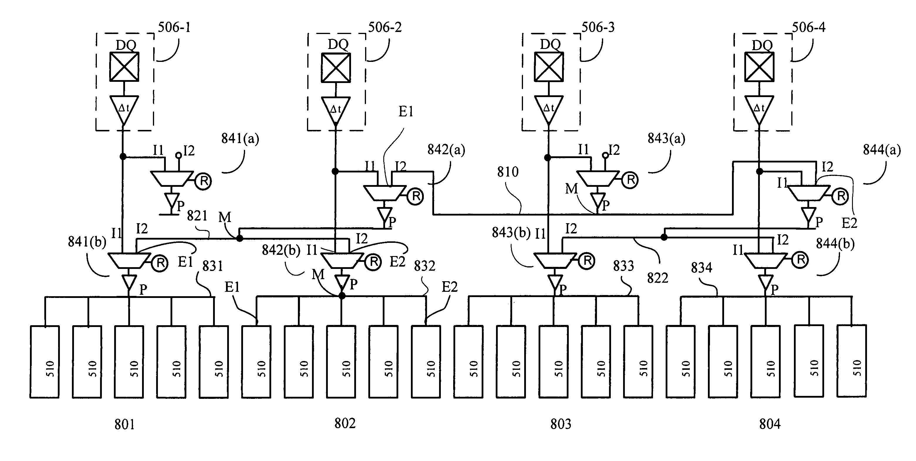
[0019]To minimize skew and to accommodate memories having different data bus widths and data group sizes, the present invention provides a modular multiple-data-rate memory I / O architecture having a balanced configurable tree structure that can be readily replicated and scaled. For illustrative purposes, the invention is described in the context of a double-data rate (DDR) system. It is to be understood, however, that the principles of this invention can be applied to a variety of multiple data rate systems.
[0020]FIG. 2A is a block diagram of an exemplary system 200 including a memory interface circuit (interface) 210, and a multiple-data rate memory device 220, according to one embodiment of the present invention. System 200 may be part of a larger system 201, such as a data processing system, which may include one or more of the following components: a processor 230, peripheral devices 240, and input / output (I / O) device(s) 250, in addition to the components in system 200. The abov...
PUM
 Abstract
Description
Claims
Application Information