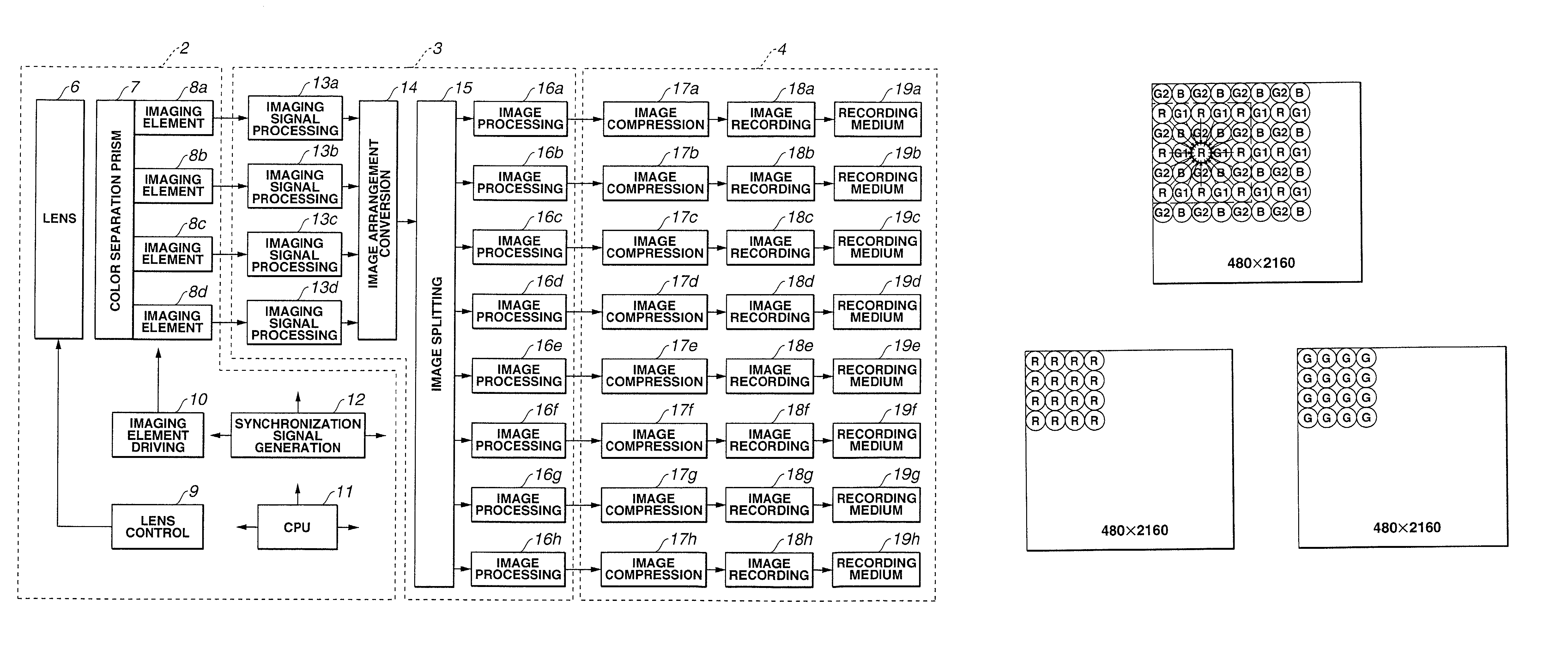
Image processing device
a processing device and image technology, applied in the field of image processing devices, can solve the problems of difficult to realize the processing speed of current image processing devices, and the difficulty of recording high-definition images obtained by such image-picking means at a moving image rate, and achieve the effect of high speed
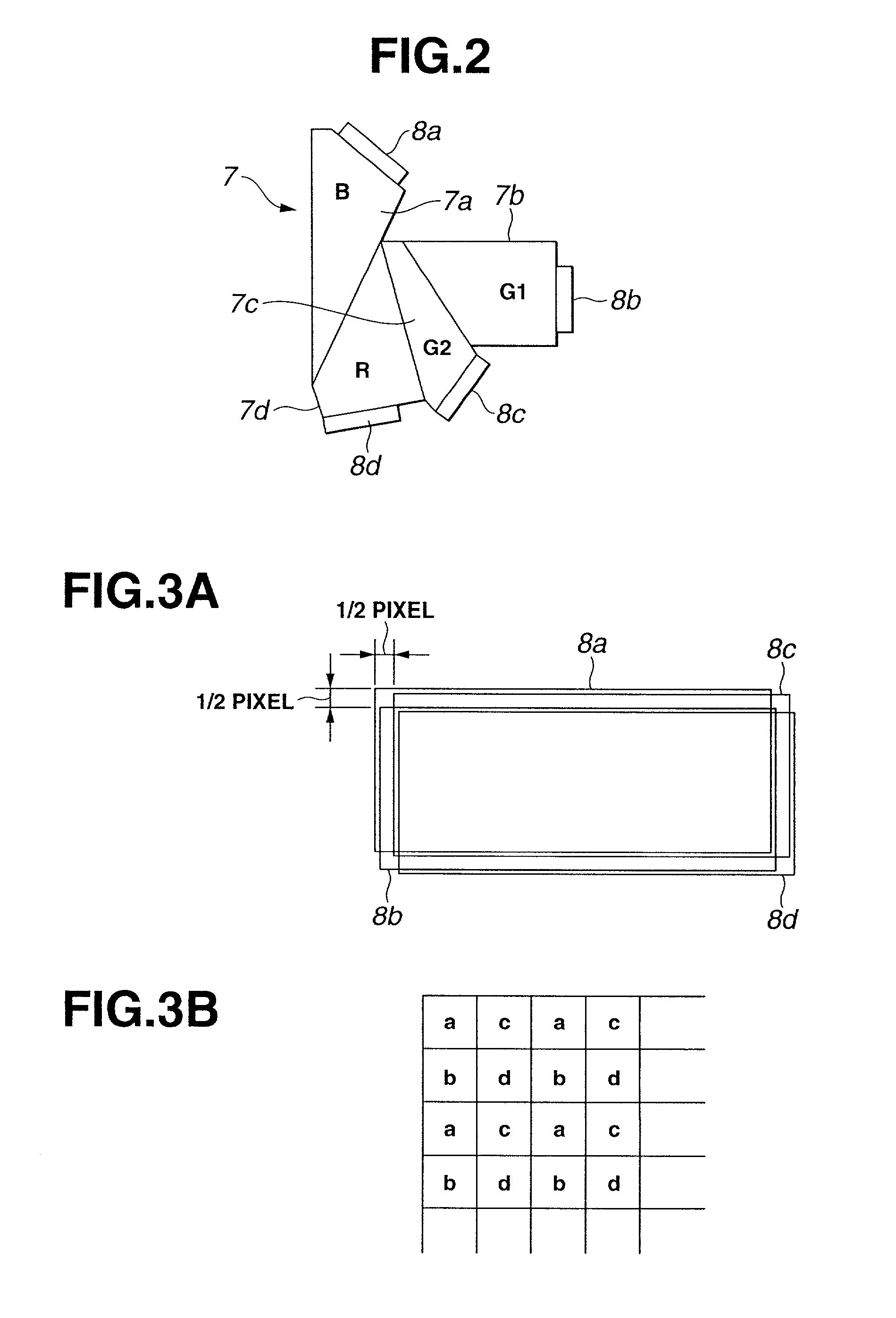
- Summary
- Abstract
- Description
- Claims
- Application Information
AI Technical Summary
Benefits of technology
Problems solved by technology
Method used
Image

Examples
second embodiment
[0119]Next, the present invention will be described.
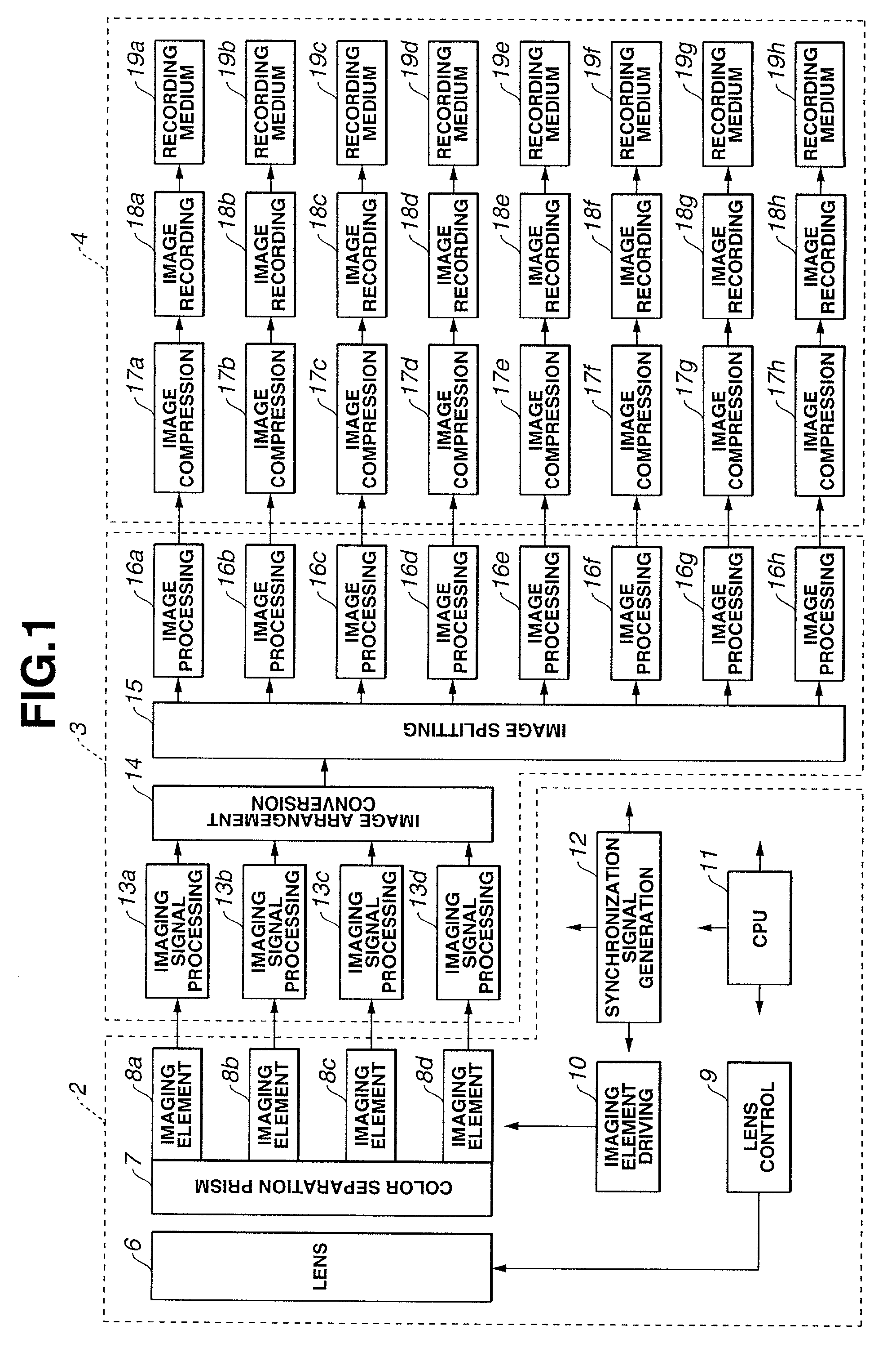
[0120]The image processing device 1B of the second embodiment shown in FIG. 9 has a configuration in which a display part 5 is further installed in the image processing device 1A shown in FIG. 1.
[0121]Specifically, the output signals of the image processing circuits 16i are input into the image conversion circuits 30i (i=a to h) of an image conversion circuit part 30 that forms a portion of the display part 5. Then, after being converted into images consisting of desired numbers of pixels by the image conversion circuits 30i, these signals are input into a display processing circuit 31, and signal processing which allows display by a display device 32 is performed, so that the signals can be displayed by this display device 32.
[0122]Furthermore, in this second embodiment, the lens 6 is constructed from a zoom lens, and the device is arranged so that the zoom magnification can be altered by operating zoom magnification altering mean...
third embodiment
[0169]Next, the present invention will be described.
[0170]FIG. 21 shows the overall configuration of the image processing device of a third embodiment of the present invention. FIG. 22 is an explanatory diagram of the function of the image synthesizing circuit.
[0171]The image processing device 1E of the third embodiment of the present invention shown in FIG. 21 has a configuration in which an image synthesizing circuit 45 which synthesizes the plurality of split images produced by the image processing circuits 16a through 16h into a single image is provided in the image processing device 1B of the second embodiment of the present invention shown in FIG. 9, and in which an image splitting circuit 46 which splits the image synthesized by the abovementioned image synthesizing circuit 45 into a plurality of images is further provided; the split images produced by the splitting performed by this image splitting circuit 46 are compressed by a plurality of image compression circuits 17a th...
fourth embodiment
[0185]Next, the present invention will be described.
[0186]FIGS. 25A, 25B and 25C show how image splitting is performed by providing a portion that partially overlaps with an adjacent split image in a fourth embodiment of the present invention. FIG. 26 is an explanatory diagram of the writing operation into the FIFO memories that make up the image splitting circuit in this case. FIG. 27 is an explanatory diagram which shows how pixels of portions that overlap pixels in the vicinity of the ends of the respective split image regions are utilized in image processing.
[0187]The image processing device of this fourth embodiment has the same configuration as (for example) the image processing device 1A shown in FIG. 1, but differs from this image processing device 1A in that image splitting is performed by providing a portion that partially overlaps with an adjacent split image as described below.
[0188]Specifically, for example, eight image regions {circle around (1)} through {circle around...
PUM
 Abstract
Description
Claims
Application Information