Memory defect detection and self-repair technique

a memory defect and self-repair technology, applied in the field of memory defect detection and self-repair technique, can solve the problems of block erase operation failure, unscreenable latent manufacturing defects, and high cost of current solutions

Active Publication Date: 2007-02-13
INTEL NDTM US LLC
View PDF13 Cites 4 Cited by
  • Summary
  • Abstract
  • Description
  • Claims
  • Application Information

AI Technical Summary

Problems solved by technology

Unscreenable latent manufacturing defects may be introduced during device fabrication.
These defects may eventually break down and cause shorts in the flash memory array during customer use causing, for example, block erase operations to fail.
Current solutions can be costly and often result in only partial reduction of these defects.

Method used


Image

  • Memory defect detection and self-repair technique
  • Memory defect detection and self-repair technique
  • Memory defect detection and self-repair technique

Examples


Embodiment Construction

)

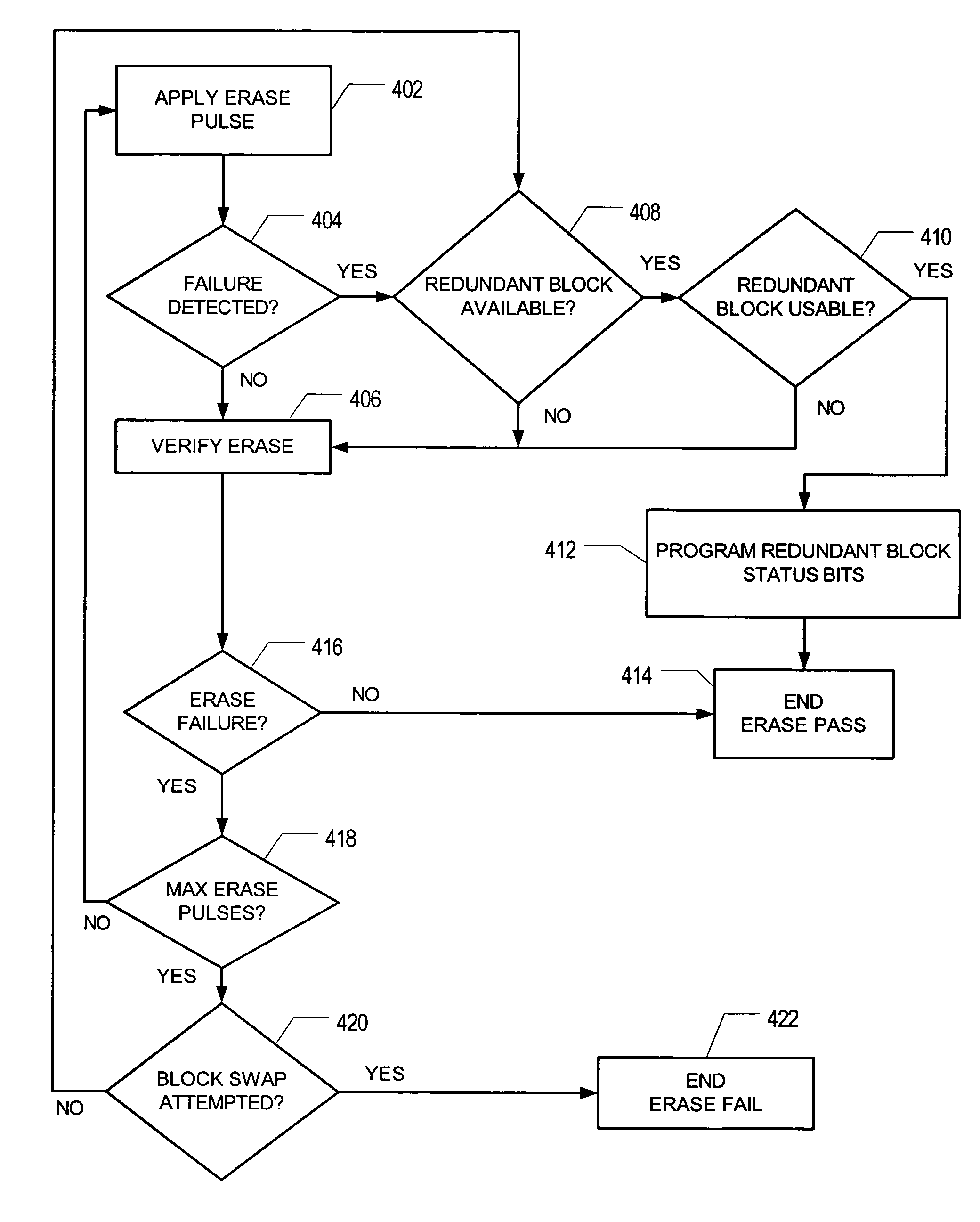
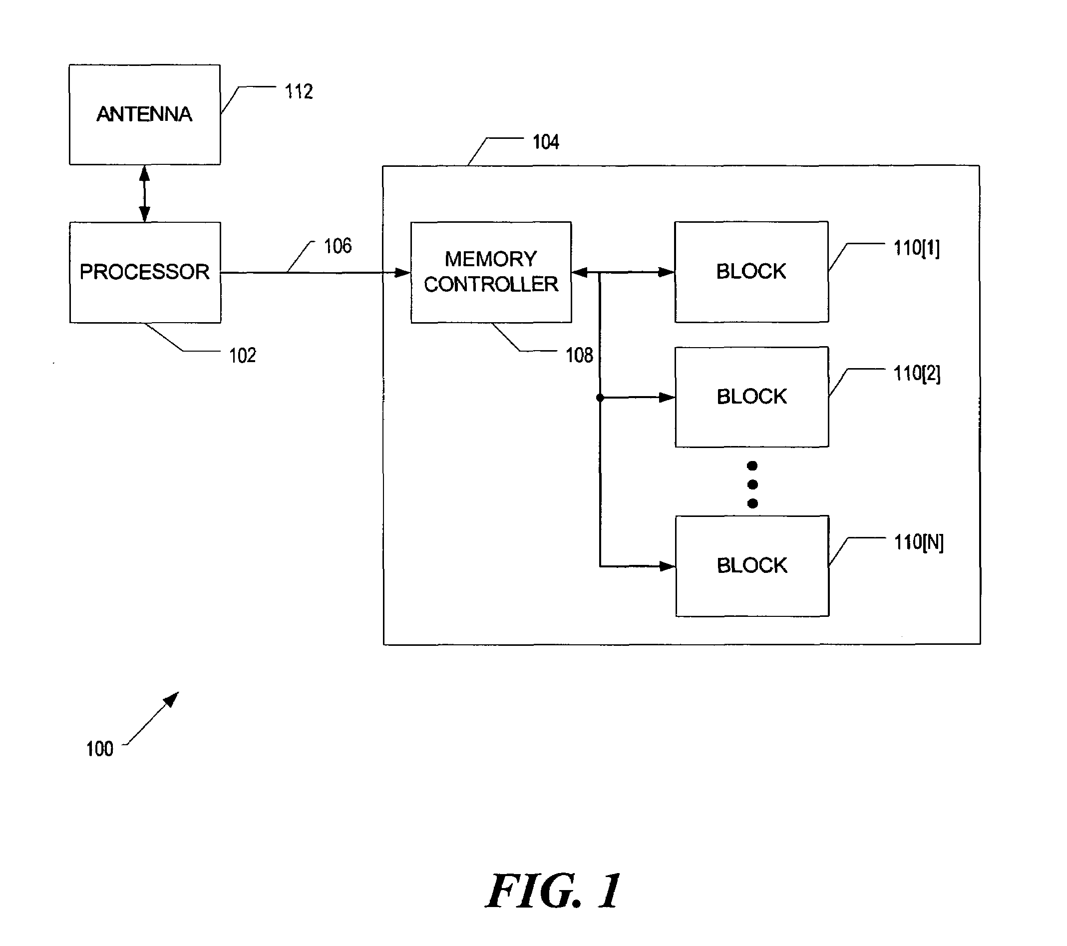
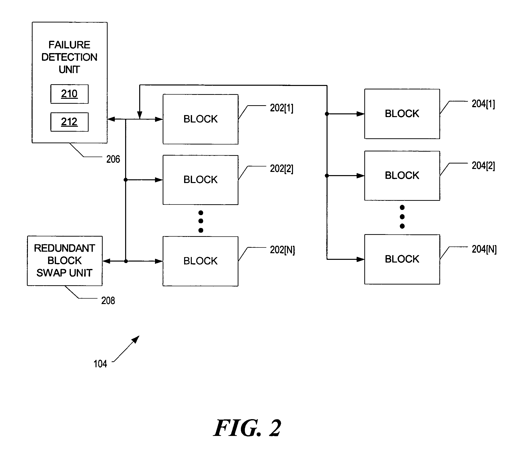
[0010]According to some embodiments, a memory device having multiple memory units includes one or more redundant memory units. Upon detection of an electrical characteristic indicating a failing memory unit, one of the redundant memory units is used to replace the failing memory unit. Detection of failing memory units may be via current, voltage and / or resistance monitoring. If the electrical characteristic monitored exceeds a predetermined threshold, a memory unit is considered failing. The failing memory unit is removed from further use. The redundant memory unit is programmed to be accessible at the memory address of the removed memory unit. Replacement occurs automatically (that is, without user intervention).

[0011]In the following description, numerous specific details are set forth. However, it is understood that embodiments of the invention may be practiced without these specific details. In other instances, well-known methods, structures and techniques have not been shown i...


PUM


Abstract

According to some embodiments, a memory device having multiple memory units includes one or more redundant memory units. Upon detection of an electrical characteristic indicating a failing memory unit, one of the redundant memory units is used to replace the failing memory unit. Detection of failing memory units may be via current, voltage and / or resistance monitoring. If the electrical characteristic monitored exceeds a predetermined threshold, a memory unit is considered failing. The failing memory unit is removed from further use. The redundant memory unit is programmed to be accessible at the memory address of the removed memory unit. Replacement occurs automatically (that is, without user intervention).

Description

BACKGROUNDDescription of the Related Art[0001]Flash memory provides a non-volatile fast-access storage medium that may be rewritten in-circuit after first erasing old data. A flash memory cell is a small memory unit utilizing, for example, a modified metal-oxide semiconductor (MOS) transistor structure. Electric charge is stored on an insulated gate positioned between the transistor's select gate and channel. The charge on the insulated gate modulates the transistor's threshold voltage (Vt), which is resolved into data states during read operations. The flash memory cell is electrically erasable.[0002]A flash memory block is a grouping of flash memory cells that are individually addressable. Due to the characteristics of flash memory, data is erased in blocks, which are typically between 8 kilobytes (KB) and 256 KB in size. Once data has been written into a particular byte location, that data cannot be changed without first erasing the byte, which requires erasing the entire block i...

Claims


Application Information

Patent Timeline
Patent Type & Authority Patents(United States)
IPC IPC(8): G11C11/34G11C16/34G11C29/00G11C29/50G11C29/52
CPCG11C29/4401G11C29/52G11C29/82G11C29/76G11C2029/0409
Inventor LINDE, REED A.SMIDT, ALEC W.
Owner INTEL NDTM US LLC
Why Eureka
Try Eureka