Method of operating a flash memory device

a flash memory and device technology, applied in the direction of digital storage, semiconductor devices, instruments, etc., can solve the problems of difficult integration nor flash memory devices, the threshold voltage of respective string selection and ground selection transistors is not readily controllable, and the nand flash memory devices comprising string selection transistors and ground selection transistors tend to malfunction frequently

Inactive Publication Date: 2007-02-13
SAMSUNG ELECTRONICS CO LTD
View PDF8 Cites 38 Cited by
  • Summary
  • Abstract
  • Description
  • Claims
  • Application Information

AI Technical Summary

Problems solved by technology

It is difficult to integrate NOR flash memory devices because a contact hole must be formed in the source / drain region of each constituent cell transistor.
However, since the string selection transistor and the ground selection transistor each comprise but a single gate electrode without a floating gate electrode or a dielectric layer, the respective threshold voltages of the string selection and ground selection transistors are not readily controllable.
Thus, a NAND flash memory device comprising the string selection transistor and the ground selection transistor tends to malfunction frequently.
Particularly, when the threshold voltages of the string selection transistor and the ground selection transistor are low, the string selection transistor and the ground selection transistor undesirably turn on, so the NAND flash memory device tends to malfunction frequently.
However, since the ion implantation process constitutes an additional fabrication step, otherwise unneeded in the formation of the NAND flash memory device cell transistors, and since the ion implantation is conventionally performed on a substrate region in which the string selection and ground selection transistors are formed, the conventional remediation scheme addressing the malfunctioning problem inhibits the integration of conventional NAND flash memory devices.
As a result, the threshold voltages associated with the string selection and ground selection transistors are not readily controllable, so the conventional NAND flash memory device has inferior electrical reliability.

Method used


Image

  • Method of operating a flash memory device
  • Method of operating a flash memory device
  • Method of operating a flash memory device

Examples


Embodiment Construction

[0020]Throughout this description of exemplary embodiments, it is understood that when an element or layer is referred to as being “on” or “connected to” another element or layer, it may be formed directly on, or connected directly to the other element, or the element or layer may be formed on or connected to another element or layer through intervening elements or layers. In contrast, when an element is referred to as being “directly on” or “directly connected to” another element or layer, there are no intervening elements or layers present.

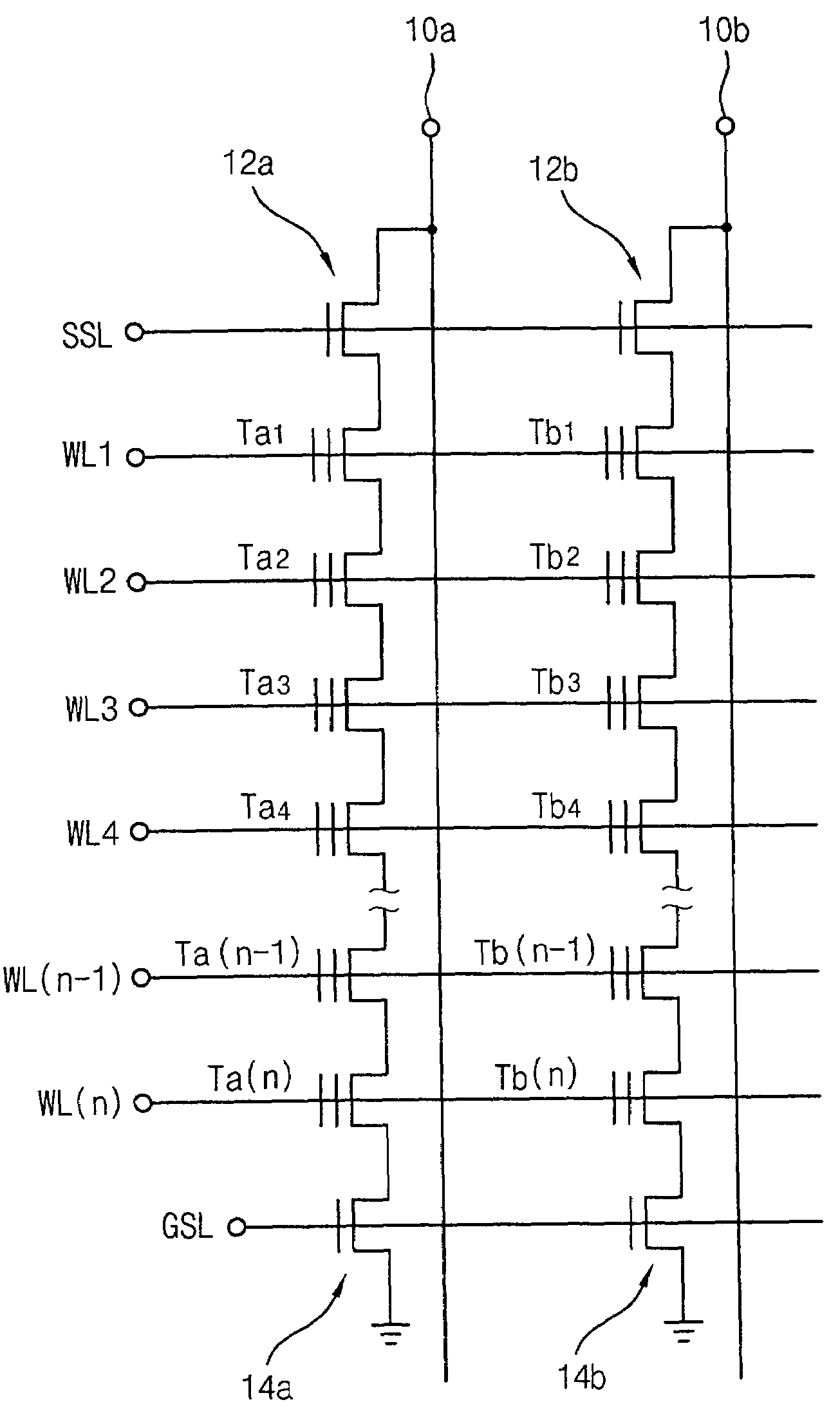
[0021]FIG. 1 is a circuit diagram of an exemplary circuit adapted for use with a method of operating a flash memory device in accordance with one embodiment of the present invention.

[0022]Referring to FIG. 1, the exemplary NAND flash memory device comprises two unit strings. A first unit string comprises string selection transistor 12a connected to bit line 10a, cell transistors Ta1, Ta2, . . . , Ta(n−1), and Ta(n), and ground selection transist...


PUM


Abstract

A method of operating a NAND flash memory device that comprising a unit string comprising a string selection transistor connected to a bit line, a cell transistor connected to the string selection transistor, and a ground selection transistor connected to the cell transistor is provided. The method comprises applying a negative bias voltage to the string selection transistor and the ground selection transistor in a stand-by mode of the NAND flash memory device.

Description

BACKGROUND OF THE INVENTION[0001]1. Field of the Invention[0002]The present invention relates to a method of operating a flash memory device, and more particularly, to a method of operating a flash memory device that is capable of readily controlling the threshold voltages of a string selection transistor and a ground selection transistor.[0003]This application claims priority to Korean Patent Application No. 2004-93845, filed on Nov. 17, 2004, the subject matter of which is hereby incorporated by reference in its entirety.[0004]2. Description of the Related Art[0005]In general, flash memory devices are non-volatile memory devices, and have been widely used in digital cameras, computers, mobile phones, memory cards, etc. Each flash memory device can be classified as either a NOR flash memory device or a NAND flash memory device.[0006]It is difficult to integrate NOR flash memory devices because a contact hole must be formed in the source / drain region of each constituent cell transis...

Claims


Application Information

Patent Timeline
Patent Type & Authority Patents(United States)
IPC IPC(8): G11C11/34
CPCG11C16/0483H01L29/66825H01L27/11521H01L27/115H10B69/00H10B41/30G11C5/02G11C16/3404
Inventor YOON, JAE-MANCHO, EUN-SUKPARK, DONG-GUNLEE, CHOONG-HO
Owner SAMSUNG ELECTRONICS CO LTD
Why Eureka
Try Eureka