Semiconductor device with multi-staged cut side surfaces

a semiconductor and side surface technology, applied in semiconductor devices, semiconductor/solid-state device details, electrical devices, etc., can solve the problems of warping in the wafer, the inability to obtain semiconductor chips in an even thickness, and the fear of readily breaking a wafer having a thickness reduction by back-surface grinding, etc., to achieve the effect of reducing the thickness of the wafer

Inactive Publication Date: 2007-02-20
TAIWAN SEMICON MFG CO LTD
View PDF8 Cites 0 Cited by
  • Summary
  • Abstract
  • Description
  • Claims
  • Application Information

AI Technical Summary

Benefits of technology

[0013]It is preferred to carry out the resin-layer forming process and cut-groove forming process with such a brief time spacing as not to cause a problem of a warp in a semiconductor substrate (wafer), or place a resin-layer-formed semiconductor substrate in an temperature controlled environment so as not to cause a large warp in the semiconductor substrate due to a difference in thermal expansion / contraction ratio between the semiconductor substrate and the resin layer before forming a cut groove in the resin layer.
[0014]According to the invention, because a cut groove is formed in the resin layer formed on one surface of the semiconductor substrate, no warp is caused due to a difference in thermal expansion / contraction between the semiconductor substrate and the resin layer. This makes it possible to evenly grind a back surface of the semiconductor substrate in a flat state of the semiconductor device. Accordingly, with such a method of manufacturing a semiconductor device, it is possible to obtain a semiconductor substrate having a thickness desirably adjusted. Namely, the semiconductor substrate obtained is evenly thickness-reduced in both a center area and a peripheral area. By cutting the semiconductor substrate into individual semiconductor chips, obtained are thickness-reduced semiconductor chips having an even thickness.
[0015]The cut groove is preferably provided in two or more directions (e.g. orthogonal two directions) in order not to cause a warp in any direction on a plane within the semiconductor substrate.

Problems solved by technology

Accordingly, thickness reduction, if excessively pursued, leads to wafer or chip breakage during handling, thus resulting in yield.
In particular, in the present when wafer diameter has increased, there is a fear of readily breaking a wafer having a thickness reduced by back-surface grinding.
However, in the manufacturing method of the foregoing prior related art, there is a problem of causing a warp in a wafer due to a difference in thermal expansion / contraction ratio between the wafer and the resin layer in a course of forming a resin layer on a wafer back surface to back surface grinding, as exaggeratedly shown in FIG. 4.
Accordingly, it is impossible to obtain semiconductor chips in an even thickness.
In addition, there is a fear that the semiconductor chips cut from a wafer peripheral region be not thickness-reduced to a thickness as expected.

Method used


Image

  • Semiconductor device with multi-staged cut side surfaces
  • Semiconductor device with multi-staged cut side surfaces
  • Semiconductor device with multi-staged cut side surfaces

Examples


Embodiment Construction

[0027]Explanation will be made in detail below on an embodiment of the present invention with reference to the accompanying drawings.

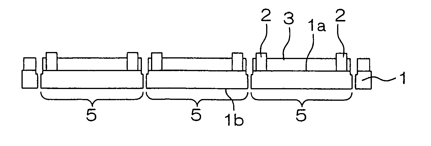
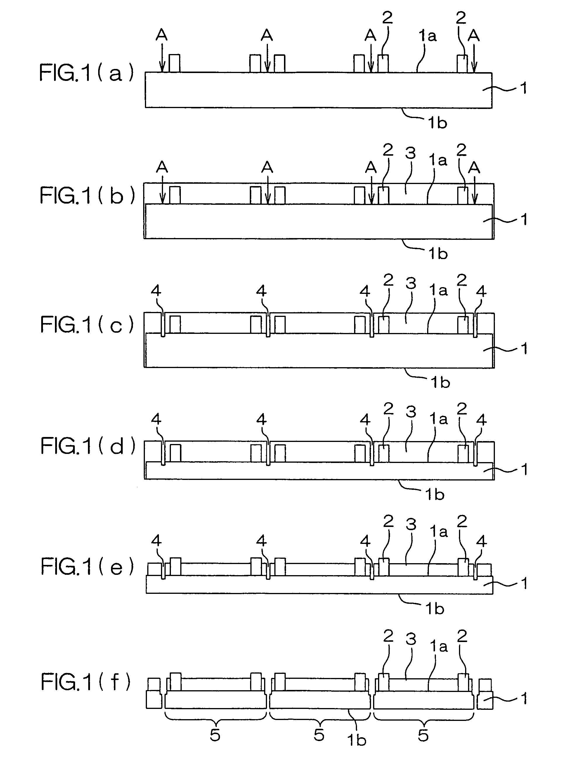
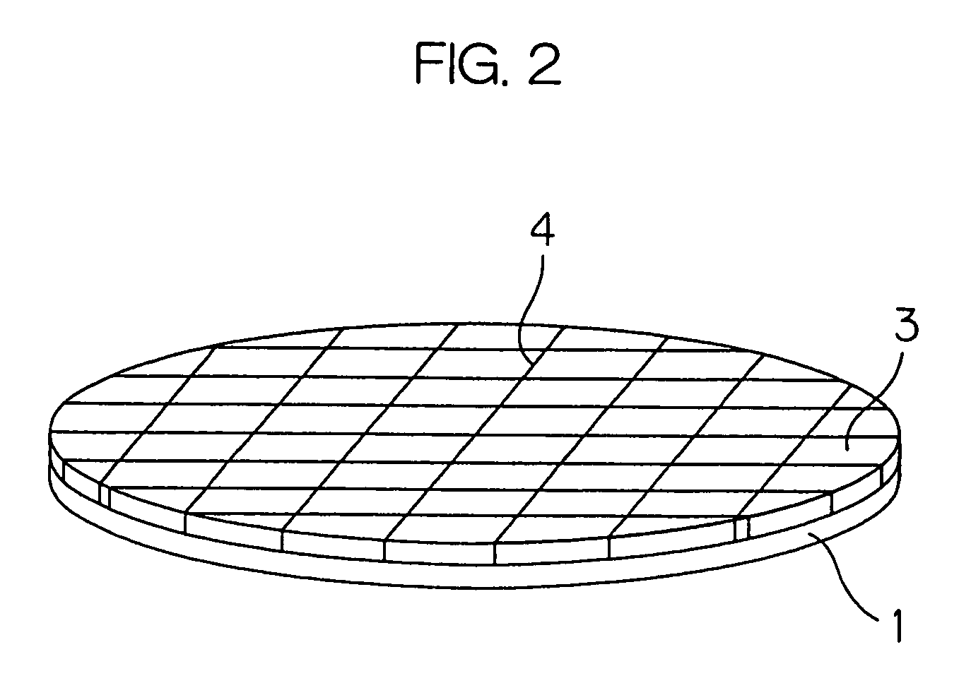
[0028]FIG. 1 is an illustrative sectional view showing, in a process sequence, a method of manufacturing a semiconductor device according to an embodiment of the invention. The semiconductor wafer 1 of FIG. 1 (hereinafter, referred merely to as a “wafer 1”), processed through various device-forming and wiring processes, has a surface 1a, as an activation surface, covered with a protection film (passivation film) of a silicon nitride film or the like. The pads for external electric connection are exposed from the protection film.

[0029]As shown in FIG. 1A, a plurality of projection electrodes 2, e.g. of gold (Au), are respectively formed on the pads. The projection electrodes 2 are preferably formed, for example, by electroplating to a height, e.g. of 50 μm, with respect to the surface of protection film. The projection electrode 2 is preferably in the f...


PUM


Abstract

A method for manufacturing a semiconductor device which enables favorable back-surface grinding of a semiconductor substrate with preventing a warp in the substrate, thereby manufacturing a thickness-reduced semiconductor device. A projection electrode is formed on a surface of a wafer. A resin layer is formed on the wafer surface to a thickness to bury a top of the projection electrode. A cut groove is formed in the resin layer along a scribe line formed on the wafer. Thereafter, grinding is made on a back surface of the wafer by the use of a grinder or the like. A surface portion of the resin layer is removed by etching or the like, to expose the top of the projection electrode. The wafer is cut along the cut groove to obtain individual semiconductor chip pieces.

Description

[0001]This is a Divisional of U.S. application Ser. No.: 10 / 192,655, filed Jul. 11, 2002, now U.S. Pat. No. 6,818,550.BACKGROUND OF THE INVENTION[0002]1. Technical Field of the Invention[0003]This invention relates to a semiconductor device and method for manufacturing the same.[0004]2. Description of the Prior Art[0005]In order to reduce a semiconductor chip thickness, conventionally the back-surface grinding process has been carried out to grind a back surface of a semiconductor wafer after having formed devices and interconnections (hereinafter, referred to merely as a “wafer”). The back-surface grinding process has been carried out by bonding a soft protection film on a wafer surface and pressurizing the wafer via the film to urge the wafer at its back surface onto a grid stone so that the wafer is rotated in that state.[0006]However, the wafer or chip is handled by a robot in a process after grinding, i.e. in a process to cut a wafer into chips or a process to mount the cut chi...

Claims


Application Information

Patent Timeline
Patent Type & Authority Patents(United States)
IPC IPC(8): H01L23/544H01L23/29H01L23/48H01L21/301H01L21/68H01L29/06
CPCH01L21/6835H01L21/6836H01L24/27H01L29/0657H01L2221/68327H01L2221/6834Y10S438/977H01L2224/274H01L2924/01078H01L2924/01079H01L2924/3511H01L2224/16
Inventor SHIBATA, KAZUTAKA
Owner TAIWAN SEMICON MFG CO LTD
Why Eureka
Try Eureka