Address coding method and address decoder for reducing sensing noise during refresh operation of memory device

a memory device and address decoding technology, applied in the field of semiconductor memory devices, can solve problems such as data loss, over-allocation of normal operation time, and increase the time consumed by memory controllers for requesting refresh operations

Active Publication Date: 2007-02-20
SAMSUNG ELECTRONICS CO LTD
View PDF7 Cites 34 Cited by
  • Summary
  • Abstract
  • Description
  • Claims
  • Application Information

AI Technical Summary

Problems solved by technology

If a refresh operation is not performed periodically, charge leakage from memory cells can result in data loss.
Since the refresh operation of a DRAM is generally controlled by a memory controller, and the like, a time consumed by the memory controller for requesting a refresh operation increases, and may exceed a time allocated to a normal operation.
Since the internal data paths perform complicated operations such as various calculations, amplification, and coding, the internal data paths cannot operate at a high speed such as 1.6 Gbps (or 1.6 GHz).
However, this method increases sensing noise since power consumption becomes non-uniform during the refresh operation.

Method used


Image

  • Address coding method and address decoder for reducing sensing noise during refresh operation of memory device
  • Address coding method and address decoder for reducing sensing noise during refresh operation of memory device
  • Address coding method and address decoder for reducing sensing noise during refresh operation of memory device

Examples


Embodiment Construction

[0026]Hereinafter, embodiments of the present disclosure will be described in detail with reference to the appended drawings. Like reference numbers refer to like components throughout the drawings.

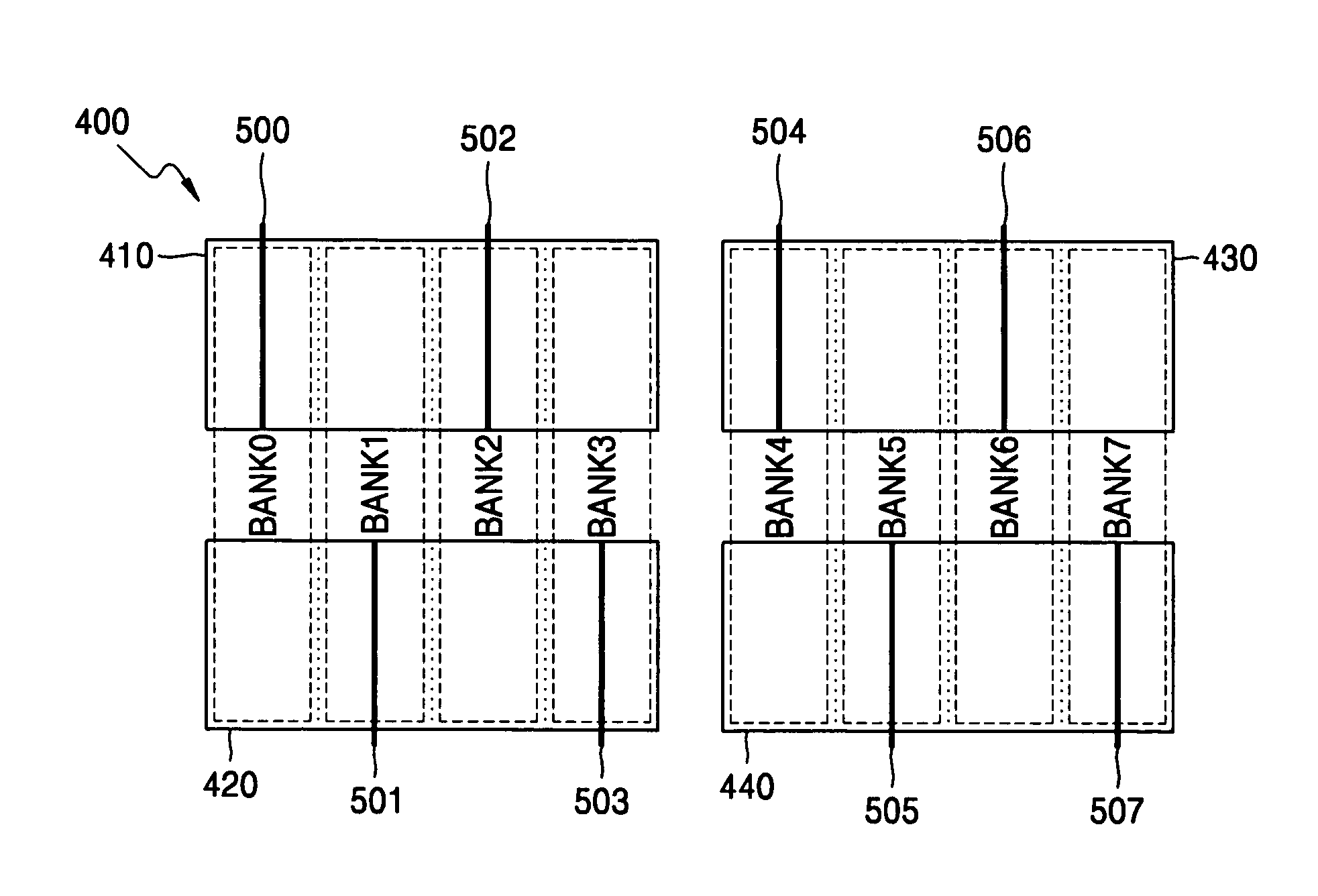
[0027]FIGS. 4a and 4b are views for explaining a memory device using a row address coding method according to an embodiment of the present disclosure. FIG. 4a is a view for explaining the row address coding method during an operation, such as a read or write operation and FIG. 4b is a view for explaining the row address coding method during a refresh operation.

[0028]Referring to FIG. 4a, as described above, an MSB of a row address signal for allocating portions of each of bank BANK0–BANK7 to one of upper and lower memory blocks 410–420 and 430–440, is RA12. Portions of banks BANK0–BANK7, within the upper first and third memory blocks 410 and 430, are addressed by a row address signal with an MSB of RA12 (“12”) and the portions banks BANK0–BANK7 within the lower second and fourth memory bl...


PUM


Abstract

An address coding method, which is performed by a memory device including a plurality of banks each being shared by at least two memory blocks, includes: activating adjacent banks shared by at least two memory blocks during a refresh operation of the memory device, and enabling the refresh operation in each bank alternately between the at least two memory blocks. The method includes activating adjacent banks shared by the at least two memory blocks during another operation of the memory device, and enabling the another operation in each bank alternately between the at least two memory blocks.

Description

BACKGROUND OF THE INVENTION[0001]This application claims priority to Korean Patent Application No. 10-2004-0072107, filed on Sep. 9, 2004, in the Korean Intellectual Property Office, the disclosure of which is incorporated herein, in its entirety, by reference.[0002]1. Field of the Invention[0003]The present invention relates to a semiconductor memory device, and more particularly, to an address coding method for reducing sensing noise during refresh and to an address decoder for performing the same.[0004]2. Description of Related Art[0005]In dynamic random access memory devices (DRAMs), periodic memory cell data refresh is important. If a refresh operation is not performed periodically, charge leakage from memory cells can result in data loss.[0006]As the capacity of DRAM increases, a time needed for refreshing increases. Accordingly, effects of increased refresh time on the performance of a DRAM system should be considered. Since the refresh operation of a DRAM is generally contro...

Claims


Application Information

Patent Timeline
Patent Type & Authority Patents(United States)
IPC IPC(8): G11C8/00
CPCG11C8/12G11C11/406G11C11/4087G11C11/40618G11C2211/4065G11C8/10
Inventor PARK, CHUL-WOO
Owner SAMSUNG ELECTRONICS CO LTD
Why Eureka
Try Eureka