Clock domain crossing FIFO

a clock domain and fifo technology, applied in the field of data communication, can solve the problems of increasing the skew concern of the over-extended clock signal, the anticipated amount of time skew between transmitted data signals, and the sensitiveness of the chip-set design to practicable limitations in terms of implementation space and available operating power

Inactive Publication Date: 2007-03-06
NXP BV
View PDF3 Cites 22 Cited by
  • Summary
  • Abstract
  • Description
  • Claims
  • Application Information

AI Technical Summary

Benefits of technology

[0015]According to another aspect of the present invention, the first processing circuit is further adapted to transmit a data control signal from the source clock domain to the storage element in the receive clock domain, the storage element being adapted to receive the data responsive to a data control signal.
[0016]The above summary is not intended to describe each illustrated embodiment or every implementation of the present invention. The figures and detailed description that follow more particularly exemplify these embodiments.

Problems solved by technology

Regardless of the configuration, the communication typically requires closely-controlled interfaces to insure that data integrity is maintained and that chip-set designs are sensitive to practicable limitations in terms of implementation space and available operating power.
This practice increases skew concerns for the over-extended clock signal.
There is often an anticipated amount of time skew between transmitted data signals themselves and between address / data signals and a clock signal at the destination.
A skew can be caused by a number of phenomena including, for example, transmission delays introduced by the capacitive and inductive loading of the signal lines of the parallel interconnect, variations in the input / output driver source, intersymbol interference and variations in the transmission lines' impedance and length.
Regardless of which phenomena cause the skew, the phenomena present a serious integrity issue for the data being communicated and, in many applications, the overall communication system.

Method used


Image

  • Clock domain crossing FIFO
  • Clock domain crossing FIFO
  • Clock domain crossing FIFO

Examples


Embodiment Construction

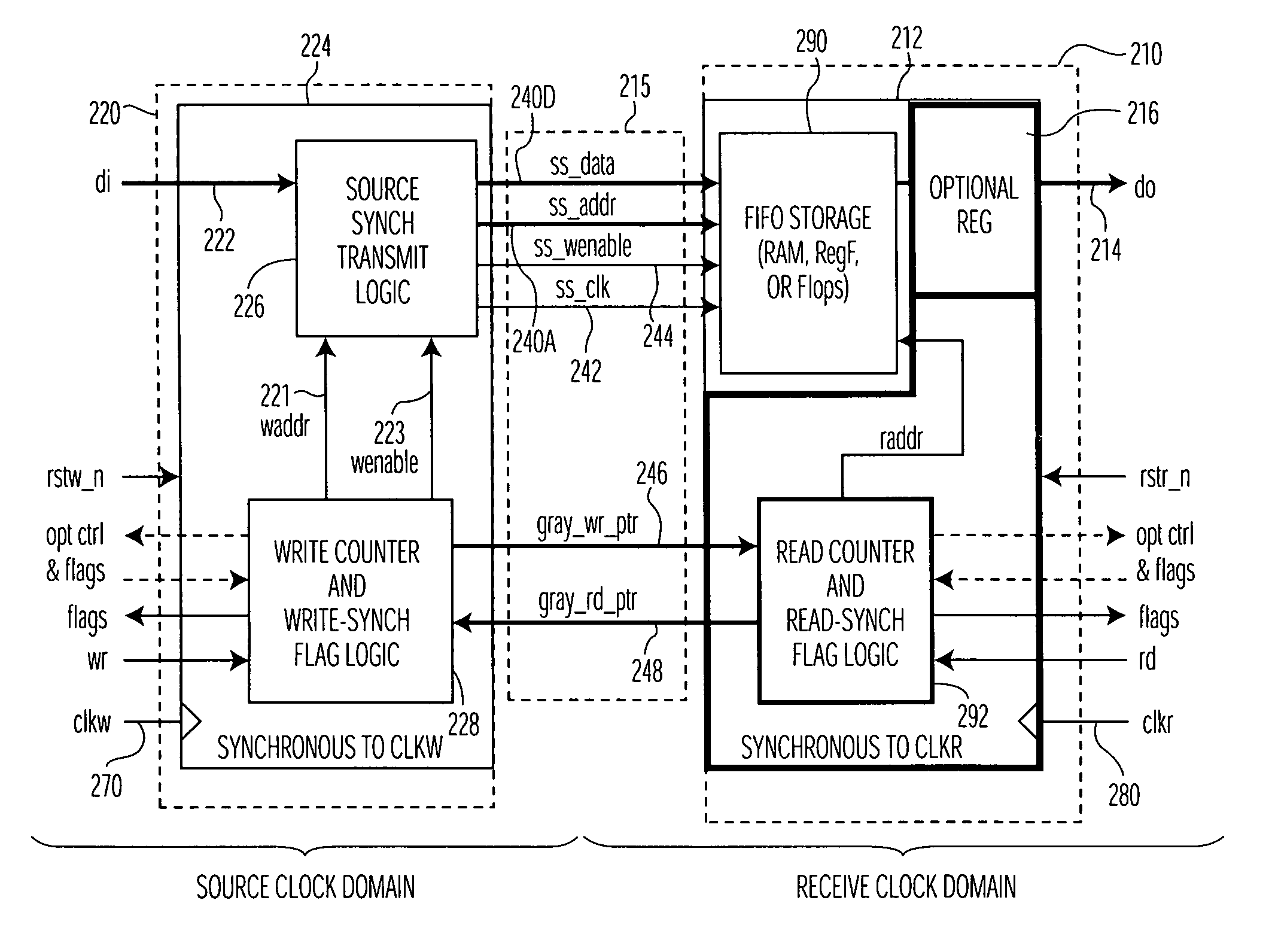
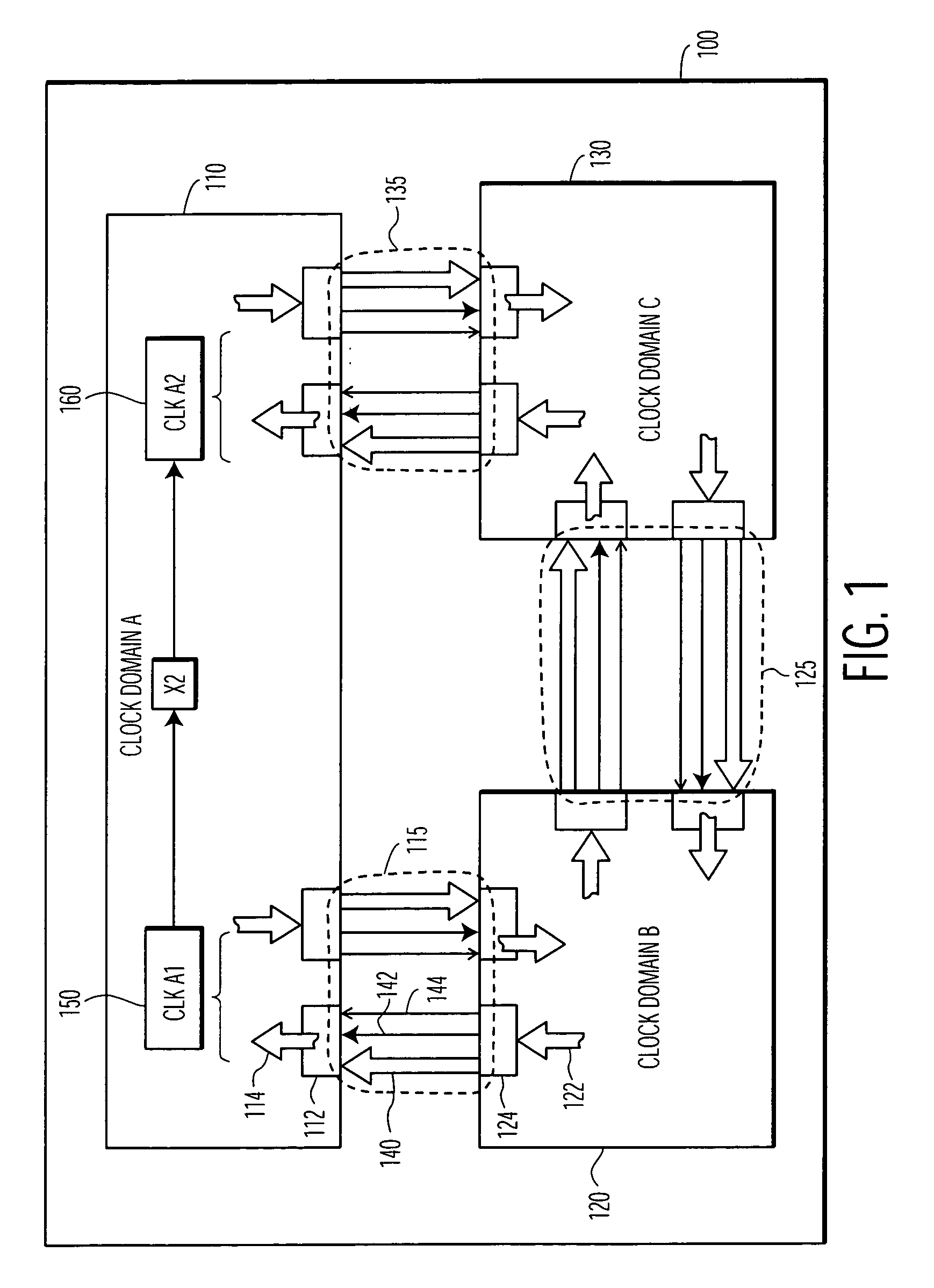
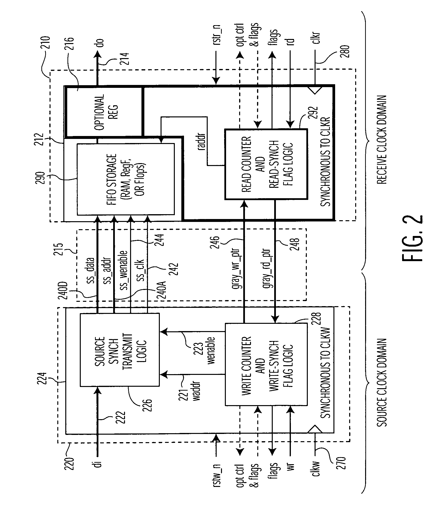
[0023]The present invention is believed to be applicable to a variety of different types of electronic circuits, and has been found to be particularly suited for use in connection with integrated circuits implemented with a plurality of clock domains and parallel data communications therebetween. While the present invention is not necessarily limited to such devices, an appreciation of various aspects of the invention is best gained through a discussion of various examples using this application.

[0024]According to a general example embodiment of the present invention, data originating from circuits within a source clock domain is transmitted through a data buffering arrangement to circuits within a receive clock domain. The data is written into the buffering arrangement synchronous with a source clock (a write clock) of the source clock domain, and read from the buffering function synchronous with a receive clock (a read clock) of the receive clock domain. The buffering arrangement ...


PUM


Abstract

A method and arrangement of passing data from a source clock domain to a non-synchronous receive clock domain are provided. A first processing circuit, located in the source clock domain, links write-address information with the data, and a clock generator generates a transmit clock signal in the source clock domain synchronous with a source clock. The first processing circuit transmits the clock signal and the data with the linked write-address information to a second processing circuit in the receive clock domain. In the receive clock domain, the second processing circuit writes the data at an address designating a storage element corresponding to the linked write-address information. The second processing circuit clocks the data into the storage element synchronous with the accompanying transmit clock signal responsive to a write enable signal from the source clock domain, and reads the data out of the storage element synchronous with a receive domain clock.

Description

FIELD OF THE INVENTION[0001]The present device relates generally to data communications and, more particularly, to methods and arrangements for transferring data between clock domain boundaries.BACKGROUND OF THE INVENTION[0002]Ongoing demands for more-complex circuits have led to significant achievements that have been realized through the fabrication of very large-scale integration of circuits on small areas of silicon wafer. These complex circuits are often designed as functionally-defined blocks that operate on a sequence of data and then pass that data on for further processing.[0003]This communication from such functionally-defined blocks can be passed in small or large amounts of data between individual integrated circuits (or “chips”), within the same chip and between more remotely-located communication circuit arrangements and systems. Regardless of the configuration, the communication typically requires closely-controlled interfaces to insure that data integrity is maintain...

Claims


Application Information

Patent Timeline
Patent Type & Authority Patents(United States)
IPC IPC(8): H04L7/00H04L25/00H04L25/40G06F5/10H04L7/02
CPCH04L7/005H04L7/02G06F5/10G06F2205/102H04L7/0008
Inventor PONTIUS, TIMOTHYPAYNE, ROBERT L.EVOY, DAVID R.
Owner NXP BV
Why Eureka
Try Eureka