
Computer-assisted electronic component schematic linking method

a technology of electronic components and schematics, applied in computing, instruments, electric digital data processing, etc., can solve problems such as easy data input errors and waste of time, erroneous schematic linking, and difficulty in distinguishing circuits and signal lines of various electronic components. to prevent erroneous schematic linking and reduce product design time

Active Publication Date: 2007-03-06
INVENTEC CORP
View PDF32 Cites 2 Cited by
  • Summary
  • Abstract
  • Description
  • Claims
  • Application Information

AI Technical Summary

Benefits of technology

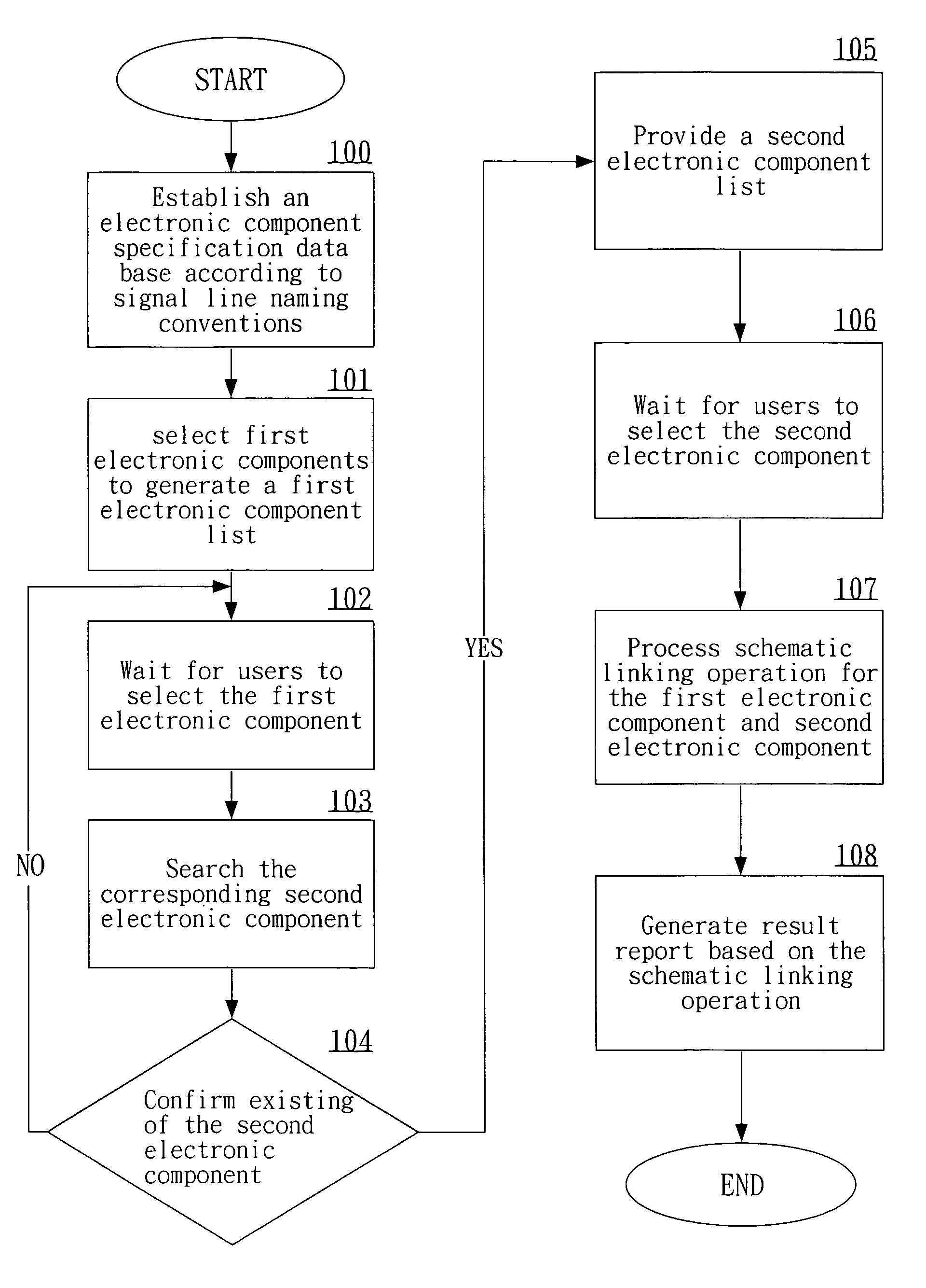
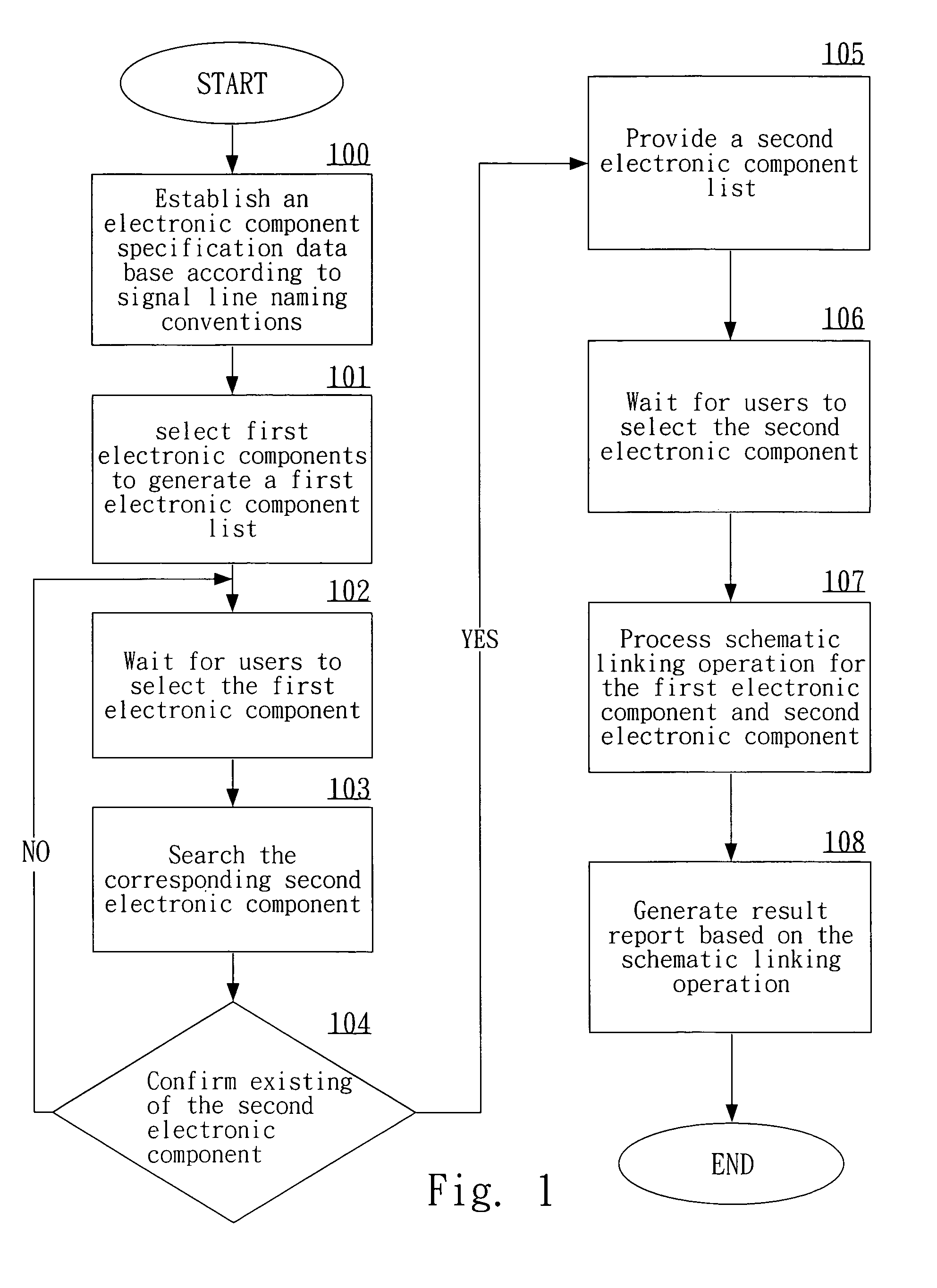
The present invention provides a computer-assisted schematic linking method for electronic components to prevent errors and reduce product design time. The method involves uniforming the naming specifications of circuits and signal lines of electronic components based on signal line naming conventions, and storing the specifications data in a database. Users can then select the first electronic component and search for the second electronic component based on the first component. The second component list is then sorted based on category for users to select. The method also includes performing a schematic linking operation of the first and second components, and generating a result report for user reference. The use of signal line naming conventions makes it easy for users to distinguish and prevent errors, and the resulting schematic module is reusable for future products, reducing design time and improving quality.

Problems solved by technology

The method mentioned above has the following drawbacks:1. As there are a great number of electronic components, even the new electronic components that are designed by modifying the similar products still could result in erroneous schematic linking.
It is easy to incur data input error and a waste of time.3. Different names of circuits and signal lines of various electronic components are difficult to distinguish.
As the product generally is jointly designed and developed by many people, the finished modules often do not have uniform standards.
This increases the difficulty of recognizing and sharing the modules.
Because of the aforesaid disadvantages, errors and waste of time on schematic chart design have been a nasty problem in the product development remained to overcome.

Method used


Image

  • Computer-assisted electronic component schematic linking method
  • Computer-assisted electronic component schematic linking method
  • Computer-assisted electronic component schematic linking method

Examples


Embodiment Construction

[0018]When engineers are in the process of product design and development, they have to link the circuits and signal lines for electronic components such as a Central Processing Unit, Random Access Memory, North Bridge chipset, South Bridge chipset, various expansion buses and the like. And schematic charts for linking the circuits and signal lines of the electronic components are made, based on product data and specifications of the electronic components. The computer-assisted schematic linking method for electronic components according to the invention aims at reducing product development time and error probability during design of the schematic charts.

[0019]FIG. 1 refers to the overall process flow. First, etablish an electronic component specification database according to signal line naming conventions (step 100). The process of setting up an electronic component database will be discussed later. Then select one or more first electronic components from the electronic component ...


PUM


Abstract

A computer-assisted schematic linking method for electronic components includes naming the circuits of various electronic components according to signal line naming conventions; storing in an electronic component specification data base; selecting a plurality of first electronic components from the electronic component data base to generate a first electronic component list for users to select the first electronic components; searching second electronic components from the electronic component data base corresponding to the selected first electronic components and generating a second electronic component list for users to select the second electronic components; processing schematic linking operation for the first electronic components and the second electronic components; and repeating the foregoing steps to select other electronic components until a complete schematic chart is finished.

Description

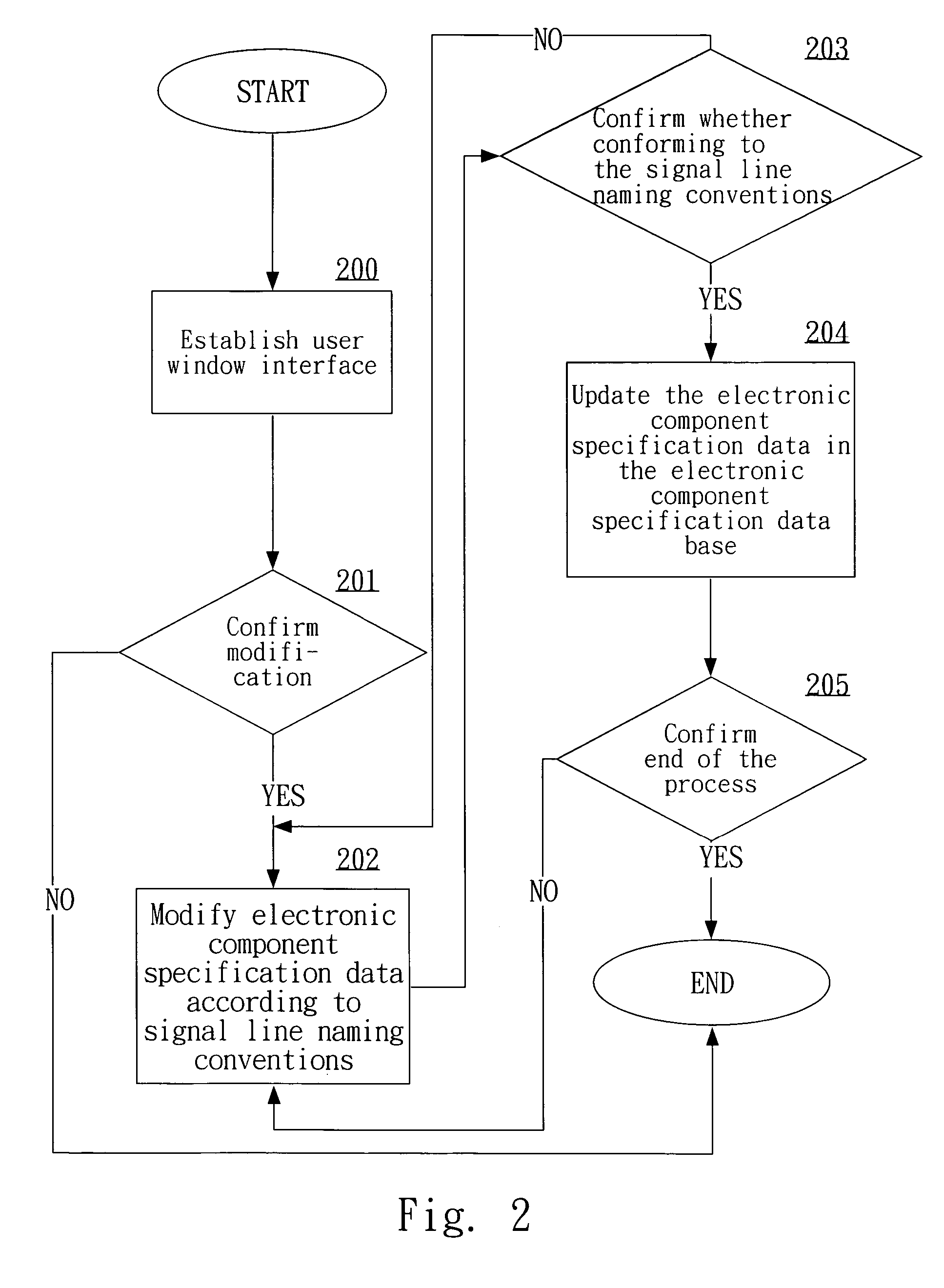
FIELD OF THE INVENTION[0001]The invention relates to a schematic linking method adopted for use in electronic information product manufacturing industries and particularly to a computer-assisted automatic linking method for schematic linking of electronic components.BACKGROUND OF THE INVENTION[0002]These days a wide variety of electronic information products are used by individuals, enterprises, and research organizations, such as a notebook computer, desktop PC, Personal Digital Assistant (PDA), server, and the like. They are deeply involved in every aspect of people's life.[0003]As the process functions of those products become more powerful, the functionality of the products also increase tremendously. And changing speed increases rapidly. It becomes very important for vendors to develop and introduce the newest products to the market place in the shortest possible time.[0004]During product design and development stage, various electronic components required in product operation ...

Claims


Application Information

Patent Timeline
Patent Type & Authority Patents(United States)
IPC IPC(8): G06F17/50
CPCG06F17/5045G06F30/30
Inventor WU, FU-CHUNGLEE, CHUN-LIANGCHEN, SHU-YUNHUANG, JUI-CHIPENG, TZE-HSINPENG, KUANG-YU
Owner INVENTEC CORP
Learn More