Method for modular design of a computer system-on-a-chip

a computer system and modular design technology, applied in the field of computer system power management, can solve the problems of large power consumption, large size and capacity, and unnecessary waiting of the computer system, so as to reduce power consumption in the computer system, minimize power consumption, and reduce the effect of computer performan

Inactive Publication Date: 2007-04-17
ST CLAIR INTPROP CONSULTANTS
View PDF17 Cites 24 Cited by
  • Summary
  • Abstract
  • Description
  • Claims
  • Application Information

AI Technical Summary

Benefits of technology

[0018]In one aspect the invention, structure and method are provided for controlling and thereby reducing power consumption in a computer system having a bus and at least one device coupled to the bus without sacrificing computer performance or inhibiting a computer user's rapid access to the computer. A unique identifier is associated with each device or resource associated with the computer, such as for example, memory, keyboard controller, mouse controller, input / output ports, and any other computer resource or peripheral. This unique identifier may typically be a device address or other device identifier such as a device serial number, network device address, and the like. Communications over a communications link such as a system or other parallel bus, serial bus, or wireless link, are monitored by each device for a predetermined time period to determine device identifiers communicated over communications link during that time period, and these identifiers (e.g. device addresses) are compared to the particular unique identifier associated or allocated to the monitoring device. Each device monitors the communications activity and is responsible for self-controlling its operating condition to minimize power consumption. Each device includes a first component which operates continuously so as to provide the monitoring functionality and a second component that operates in a low power consumption mode unless first component signals the second component that its operation is needed during that time period. The first component withholds a device operating input from the second component when none of the communicated identifiers match the particular device; and provide the device operating input to the second component when one of said communicated device identifiers match that particular device. The number of circuit components is reduced to a minimum in the first component so that the number of circuit elements which are continuously active are reduced. In one embodiment of the invention, the device operating input is a clock signal operating at the bus clock frequency. Power consumption is reduced due to the reduction in the number of circuits which are actively clocked. The inventive structure and method provide very fine temporal control of power consumption in the computer system.
[0019]In another aspect, the invention provides structure and method for a modular bus architectural (MBA) and fast modular bus architectural (FMBA) frames for System-on-a-Chip (SOC) designs including MBA / FMBA library modules that decrease design time. In another aspect, the invention provides structure and method for adjusting bus clock speed in accordance with bus activity and task performance requirements so that further control of power consumption in the system is achieved without sacrificing performance. In one embodiment, the clock rate is adjusted in accordance with preassigned performance factors associated either with a functional unit or with a task type so that the task completes within a desired time without unnecessary power consumption. In another aspect, the FMBA / MBA is provided with a configurable interface that provides alternative single-edge and double-edge First-In-First-Out buffers. Among other advantages, these FIFO structures permit interconnection of MBA / FMBA modules at the core logic level, MBA / FMBA block level, and chip level so that systems are readily and reliable designed and implemented with minimum redesign.

Problems solved by technology

The need for power management is particularly acute for battery-operated single-chip microcomputer systems, where the desirability or requirement for overall reduction in physical size (and / or weight) also imposes severe limits on the size and capacity of the battery system, and yet where extending unit operating time without sacrificing performance is a competing requirement.
Centralized power management architecture, such as that exemplified by the system in FIG. 1, has the disadvantage that, when the system is operating in a reduced power consumption state, an access to any unmasked system resource typically causes an exit (state transition) from that reduced power state to a higher power consumption state, and, in the worst case, it transitions to a full “ON” state independent of the access required.
Furthermore, since, in conventional systems, the finest timer resolution is typically controlled by the preset or programmed “idle” times which are measured and / or implemented in the millisecond or longer ranges, the computer system may need to wait unnecessarily to return to a lower power consumption or power saving state, even when access to a system resource is no longer required, or the required access cannot be made during a particular time interval due to multitasking constraints.
A further disadvantage from such conventional systems, is that system resource components receiving the bus clock continue to receive the bus clock signals at all times independent of any actual access to that resource, and that such signals are propagated to each and every component of the system.
Because several hundred or several thousand gates are dynamically switching in response to the bus clock triggered transitions, independent of the actual access by the system of the resource, substantial power is consumed unnecessarily.
This switching loss is particularly disadvantageous in current CMOS-based implementations where static operation has a much lower power consumption than dynamically switched operations.
A further disadvantage of conventional systems which results in increased power consumption, pertains to the structure of the bus-to-device-interface interposed between a system bus and a particular system component.
A further disadvantage of conventional systems, particularly for software-based power management, is the delay associated with initiating access to a device which has been placed in a lower power consumption state.
Once a device is placed in a reduced power consumption state, significant time delays (for example, delays on the order of tens of hundreds of micro seconds (10−6 seconds) may be required to reconfigure the device for access.

Method used


Image

  • Method for modular design of a computer system-on-a-chip
  • Method for modular design of a computer system-on-a-chip
  • Method for modular design of a computer system-on-a-chip

Examples


Embodiment Construction

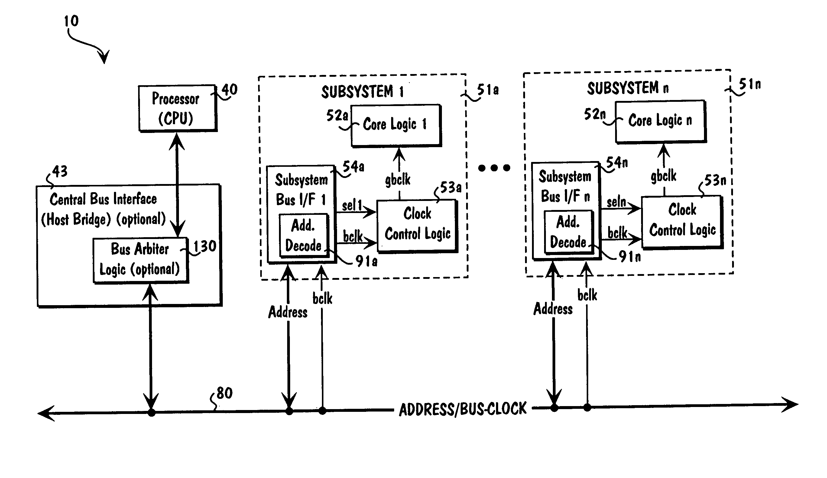
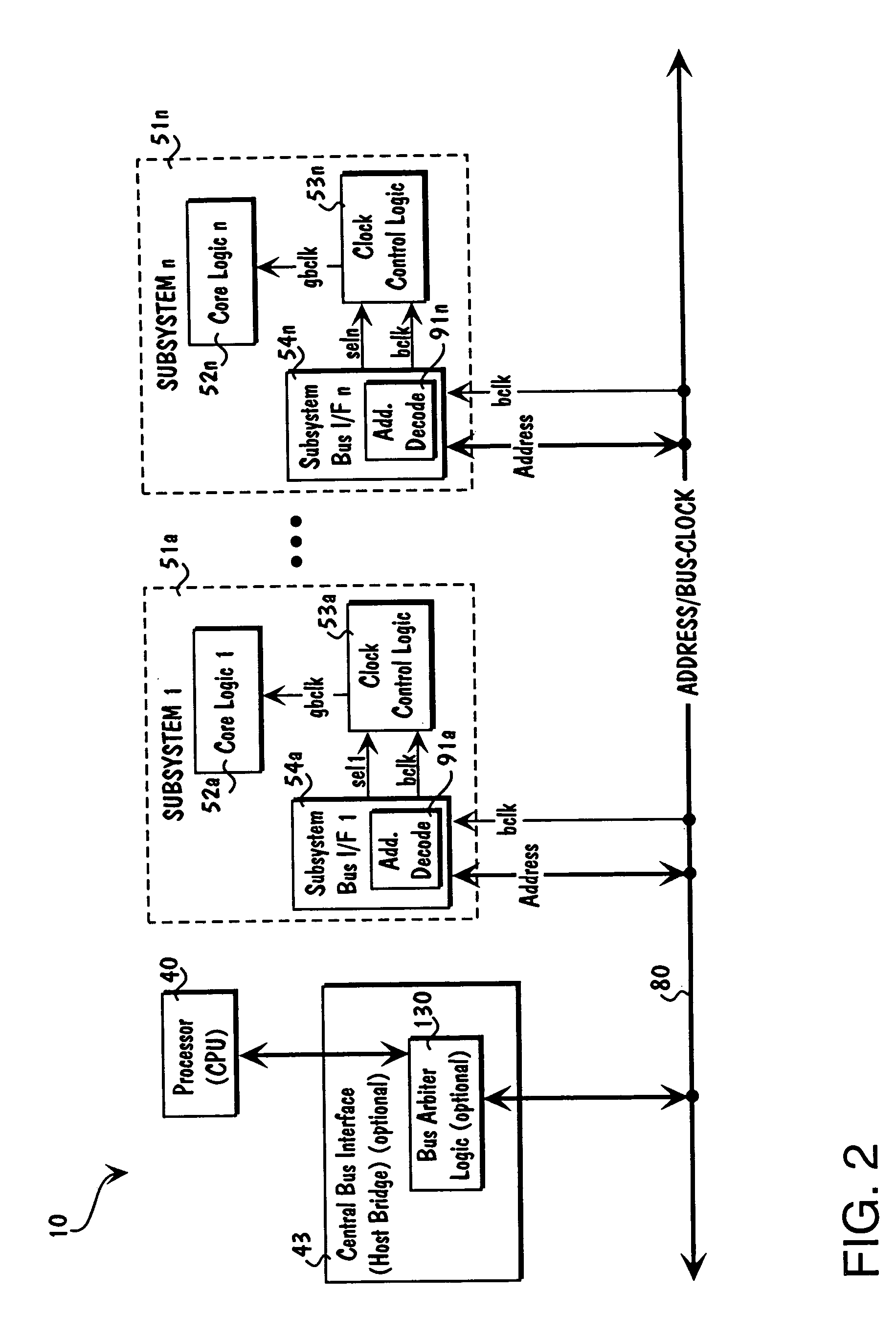
[0068]The inventive distributed power management system (DPMS) and method (DPMM) is now described with respect to the exemplary implementation of a computer system 10 in FIG. 2. A host processor, microprocessor, or central processing unit (CPU) 40 (such as made by Intel, Advanced Micro Devices, Cyrix, Motorola, Apple Computer, for example) is coupled to the other system components via central or main system bus 80 which propagates control and data signals including bus clock signals (bclk) and address signals (add). An optional host CPU-to-central bus interface 43 (referred to as a host bridge) may also be provided to accept signals from CPU 40 over a host bus 41, and translate, reformat, adjust timing, or the like processing of these signals, prior to placing them on the system bus 80 (See FIG. 3 for additional details). Such bus interface 43 may optionally but advantageously be provided as a bridge circuit so that CPU 40 may be modified or replaced by alternative designs without r...


PUM


Abstract

In a computer system having a device and a communications link for communicating with the device. A method for dynamically managing power consumption by the computer system comprises associating a particular device identifier with the device. Communications are monitored over the communications link to determine whether the communications include the particular device identifier. A clock input is withheld from the device when the communications do not include the particular device identifier. Clock input is provided to the device only when the communications include the particular device identifier. The clock input causes the device to transition from a non-operational power conservative state to an operational state wherein the device consumes more power than in the non-operational state. A performance requirement is established for a task to be executed. Clock frequency is dynamically controlled according to the performance requirement established for the task being executed.

Description

RELATED APPLICATIONS[0001]This patent application is a divisional of U.S. patent application Ser. No. 09 / 570,318 filed on May 12, 2000, now U.S. Pat. No. 6,813,674, which is a divisional of U.S. patent application Ser. No. 09 / 376,271 filed on Aug. 18, 1999, now U.S. Pat. No. 6,115,823, which is a continuation-in-part application of U.S. patent application Ser. No. 08 / 877,140 filed Jun. 17, 1997, now U.S. Pat. No. 5,987,614, all of which are hereby incorporated by reference in their entirety.FIELD OF THE INVENTION[0002]This invention pertains generally to the field of computer system power management, and more particularly to a distributed power management system and method wherein power management functions are delegated to individual modular subsystems or functional components within the overall computer system.BACKGROUND OF THE INVENTION[0003]Power management has been, and continues to be, a major concern in the development and implementation of battery powered or battery operated...

Claims


Application Information

Patent Timeline
Patent Type & Authority Patents(United States)
IPC IPC(8): G06F17/50G06F1/32
CPCG06F1/3203G06F1/3237G06F1/324G06F1/325G06F1/3259G06F1/3271G06F1/3275G06F1/3228Y02B60/148Y02B60/1217Y02B60/1221Y02B60/1225Y02B60/1253Y02B60/1257Y02B60/1228Y02D10/00
Inventor VELASCO, FRANCISCOPHUNG, XUYEN N.MITCHELL, PHILLIP M.FUNG, HENRY T.
Owner ST CLAIR INTPROP CONSULTANTS
Why Eureka
Try Eureka