Low profile wire bond for an electron sensing device in an image intensifier tube

an electron sensing device and electron sensing technology, which is applied in the field of low-profile wire bonding of electron sensing devices in image intensifier tubes, can solve the problems of not being able to reduce the vertical space between output surfaces, not being able to close the space between input surfaces of imagers and output surfaces previously

Inactive Publication Date: 2007-04-03
EXCELIS INC
View PDF3 Cites 54 Cited by
  • Summary
  • Abstract
  • Description
  • Claims
  • Application Information

AI Technical Summary

Problems solved by technology

Such close spacing presents a problem, because a conventional silicon die of a CMOS imager, for example, includes wires looping above the input surface of the imager for outputting the intensified image signal.
As these wires flare out from the silicon die and loop above the input surface, before they are connected to bond pads on a ceramic carrier holding the silicon die, it has not previously been possible to closely space the input surface of the imager to the output surface of the MCP.
However, because of the looping of wires 40, it is not possible to reduce the vertical space between output surface 18b and the top surface of silicon die 32.

Method used


Image

  • Low profile wire bond for an electron sensing device in an image intensifier tube
  • Low profile wire bond for an electron sensing device in an image intensifier tube
  • Low profile wire bond for an electron sensing device in an image intensifier tube

Examples


Embodiment Construction

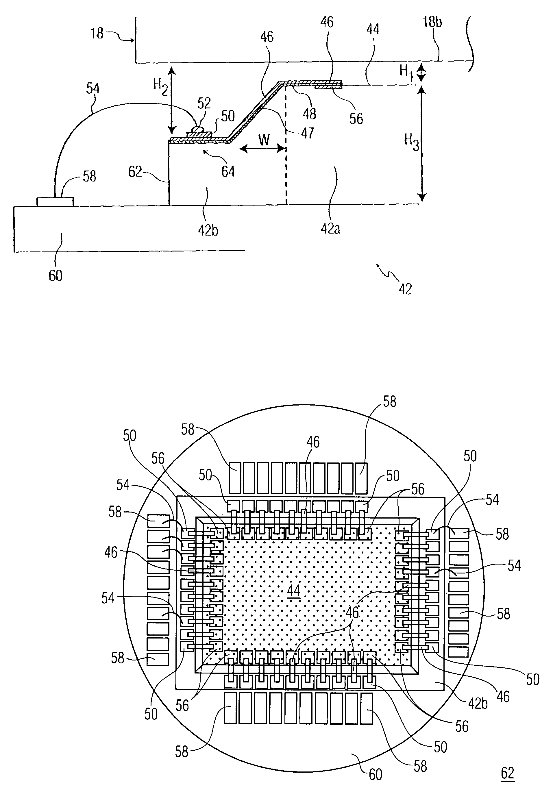
[0032]Referring to FIGS. 3a and 3b, there is shown a first embodiment of the invention. As shown, an electron sensing device, generally designated as 62, includes silicon die 42 disposed on ceramic carrier 60. Silicon die 42 includes a planar portion 42a terminating in a step portion 42b. Both the planar and the step portions are formed from silicon.

[0033]The top surface of planar portion 42a, generally designated as 44, includes an active area of the silicon die having components sensitive to light received from electron gain device 18. Active surface area 44 is placed in close vertical proximity to output surface 18b of electron gain device 18. The vertical separation between active surface area 44 and output surface 18b of the electron gain device, designated as H1, may be less than 100 microns, and typically approximately 0.0007 inches (18 microns). Accordingly, this vertical separation may be made very small with a tight clearance.

[0034]The vertical separation may be made very ...


PUM


Abstract

An electron sensing device for receiving electrons from an output surface of an electron gain device has a silicon die including an active surface area for positioning below the output surface of an electron gain device. The silicon die also includes a silicon step formed below and surrounding the active surface area, and a first array of bond pads formed on the silicon step for providing output signals from the silicon die. When the electron sensing device is positioned below the electron gain device, a tight vertical clearance is formed between the output surface of the electron gain device and the active surface area of the electron sensing device.

Description

FIELD OF THE INVENTION[0001]The present invention relates, in general, to image intensifier tubes and, more specifically, to an electron sensing device having a low profile wire bond for providing close contact in the image intensifier tube between the electron sensing device and an electron gain device, such as a microchannel plate (MCP).BACKGROUND OF THE INVENTION[0002]Image intensifying devices use solid state sensors, such as CMOS or CCD devices. Image intensifier devices amplify low intensity light or convert non-visible light into regularly viewable images. Image intensifier devices are particularly useful for providing images from infra-red light and have many industrial and military applications. For example, image intensifier tubes may be used for enhancing the night vision of aviators, for photographing astronomical events and for providing night vision to sufferers of night blindness.[0003]There are three types of image intensifying devices: image intensifier tubes for ca...

Claims


Application Information

Patent Timeline
Patent Type & Authority Patents(United States)
IPC IPC(8): H01J40/14H01J31/50H01J43/30H01L31/00
CPCH01J29/98H01J31/26H01J43/246H01J43/30H01J31/48H01L2924/10156H01L2224/02371H01L2224/48091H01L2924/10155H01L2924/00014
Inventor MEISEL, THOMAS M.THOMAS, NILS I.
Owner EXCELIS INC
Why Eureka
Try Eureka