Calculating method, verification method, verification program and verification system for edge deviation quantity, and semiconductor device manufacturing method

Inactive Publication Date: 2007-04-03
KK TOSHIBA
View PDF9 Cites 6 Cited by
  • Summary
  • Abstract
  • Description
  • Claims
  • Application Information

AI Technical Summary

Benefits of technology

[0129]FIG. 13 is a diagram for explaining a conventional method of calculating an edge deviation quantity;
[0

Problems solved by technology

However, with advancement of fine patterning, it becomes difficult to faithfully form a pattern in each process.
Thus, there occurs a problem that the finish pattern is not provided as the desired pattern.
However, with complication of the OPC and PPC techniques in recent years, a pattern produced by a device designer and a mask pattern for use during exposure are greatly different from each other, and thus, a finish pattern to be formed on a wafer cannot be easily predicted.
In particular, calculation of a trigonometric function (cos(ω−ω′)t−i sin(ω−ω′)t) expanding a portion of exp(i(ω−ω′)t) on which a great calculation load is applied is carried out two times. Thus, there has been a problem that much time is required for calculation of the trigonometric function, and an edge deviation quantity cannot be calculated with high precision for a short period of time.

Method used


Image

  • Calculating method, verification method, verification program and verification system for edge deviation quantity, and semiconductor device manufacturing method
  • Calculating method, verification method, verification program and verification system for edge deviation quantity, and semiconductor device manufacturing method
  • Calculating method, verification method, verification program and verification system for edge deviation quantity, and semiconductor device manufacturing method

Examples


example 1

[0162]As an example, by referring to FIGS. 4–6, comparison is made between a deviation quantity obtained by the method of calculating an edge deviation quantity according to the present embodiments with a deviation quantity obtained by a conventional method for calculating an edge deviation quantity, while specifying a mask pattern used.

[0163]As shown in FIG. 4, a dark field mask 21 is provided as a mask. The dark field mask 21 has a cutout pattern 22 of a rectangle of 1 μm in a direction of a long side and 0.09 μm in a direction of a short side. OPC is applied to the dark field mask 21, and using the corrected mask, a finish pattern is calculated under a condition of 193 nm in exposure light wavelength, 0.75 in numerical aperture (NA), 0.85 in coherent factor (σ), ⅔ ring band illumination (illumination center shield rate), and the reference exposure quantity Ith=0.218.

[0164]Then, a long side pattern edge of a rectangle of the design data of the mask is divided into equal intervals ...

example 2

[0169]As another example of the mask pattern, FIG. 7 shows a bright field mask 31. The bright field mask 31 has a remaining pattern 32 of a rectangle of 1 μm in a direction of a long side and 0.09 μm in a direction of a short side. Similarly to the Example 1 with reference to FIGS. 4–6, a deviation quantity obtained by the method of calculating an edge deviation quantity according to the present embodiment is compared with that of the conventional method, and a comparison result is shown in FIG. 8.

[0170]That is, a long side pattern edge of a rectangle of the design data of the mask is divided into equal intervals along the long side edge. In accordance with the method according to the present embodiment, the light beam intensity in the position coordinate of each division point and one-story differentiation of the light beam intensity are calculated, an edge deviation quantity (ΔCD1) from the design data is obtained, and the thus obtained quantity is indicated by a dotted line in FI...


PUM


Abstract

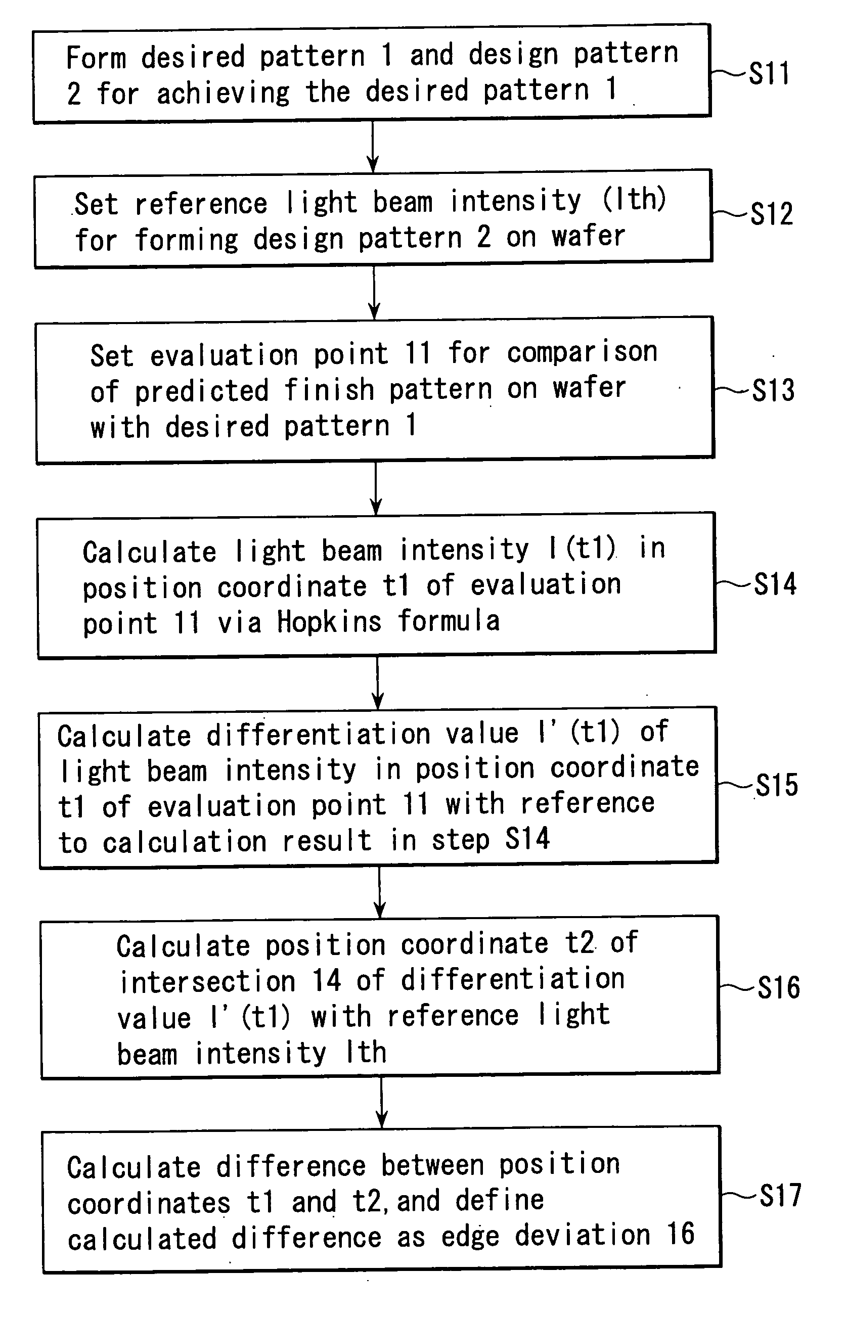
A method in which a desired pattern is compared with a finish pattern to be formed on a wafer, which is predicted from a design pattern, based on a calculation of a light beam intensity, and a deviation quantity of the finish pattern from the desired pattern at each edge of the finish pattern and the desired pattern is calculated, comprising setting a reference light beam intensity for setting the desired pattern on a wafer, setting an evaluation point for comparison of the finish pattern with the desired pattern, calculating a light beam intensity at the evaluation point, calculating a differentiation value of the light beam intensity at the evaluation point, calculating an intersection of the differentiation value with the reference light beam intensity, and calculating a difference between the intersection and the evaluation point, the difference defining an edge deviation quantity of the finish pattern from the desired pattern.

Description

CROSS-REFERENCE TO RELATED APPLICATIONS[0001]This application is based upon and claims the benefit of priority from prior Japanese Patent Application No. 2003-074821, filed Mar. 19, 2003, the entire contents of which are incorporated herein by reference.BACKGROUND OF THE INVENTION[0002]1. Field of the Invention[0003]The present invention relates to a technique for manufacturing an exposure mask for use in a light or X-ray exposure method and more particularly, the present invention relates to a calculation method, a verification method, a verification program, a verification system, and a semiconductor device manufacturing method, for an edge deviation quantity of a finish pattern from a desired pattern in order to obtain a fine pattern.[0004]2. Description of the Related Art[0005]Advancement of a semiconductor manufacturing technique in recent years is very remarkable, and a semiconductor device such as LSI whose size is 0.18 μm in minimum design rule is mass-produced. Such a fine ...

Claims


Application Information

Patent Timeline
IPC IPC(8): G06F17/50G06K9/00G03F1/36G03F1/68G03F1/70G03F7/20H01L21/027
CPCG03F7/705
InventorIZUHA, KYOKOKOTANI, TOSHIYATANAKA, SATOSHI
OwnerKK TOSHIBA