Chalcogenide memory having a small active region

a chalcogenide memory and active region technology, applied in the field of memory devices, can solve the problems of poor yield during manufacturing, excessive design power in order to switch states, and chalcogenide memories are not readily driven by cmos circuitry, etc., to achieve low power consumption, reduce the required switching energy, and high storage density

Active Publication Date: 2007-04-10
MACRONIX INT CO LTD
View PDF6 Cites 123 Cited by
  • Summary
  • Abstract
  • Description
  • Claims
  • Application Information

AI Technical Summary

Benefits of technology

[0012]The present invention is directed to overcoming problems of the prior art. In particular, the present invention may provide a design and method for fabricating phase change memory cells with small dimensions which may be below the limits of current photolithography and reduce the required switching energy. The present invention discloses a phase change memory that can have relatively low power consumption and high storage density. The present invention further discloses a method of making a phase change memory having relatively small device features.

Problems solved by technology

Unfortunately, the small holes can be difficult to fabricate and fill, potentially resulting in poor yields during manufacturing.
Chalcogenide memories are not readily driven by CMOS circuitry due to the relatively high current requirements needed to change phases.
Such prior art designs can consume an excessive amount of power in order to switch states, with the active regions of the prior art memory cells having been relatively large and difficult to fabricate.

Method used


Image

  • Chalcogenide memory having a small active region
  • Chalcogenide memory having a small active region
  • Chalcogenide memory having a small active region

Examples


Embodiment Construction

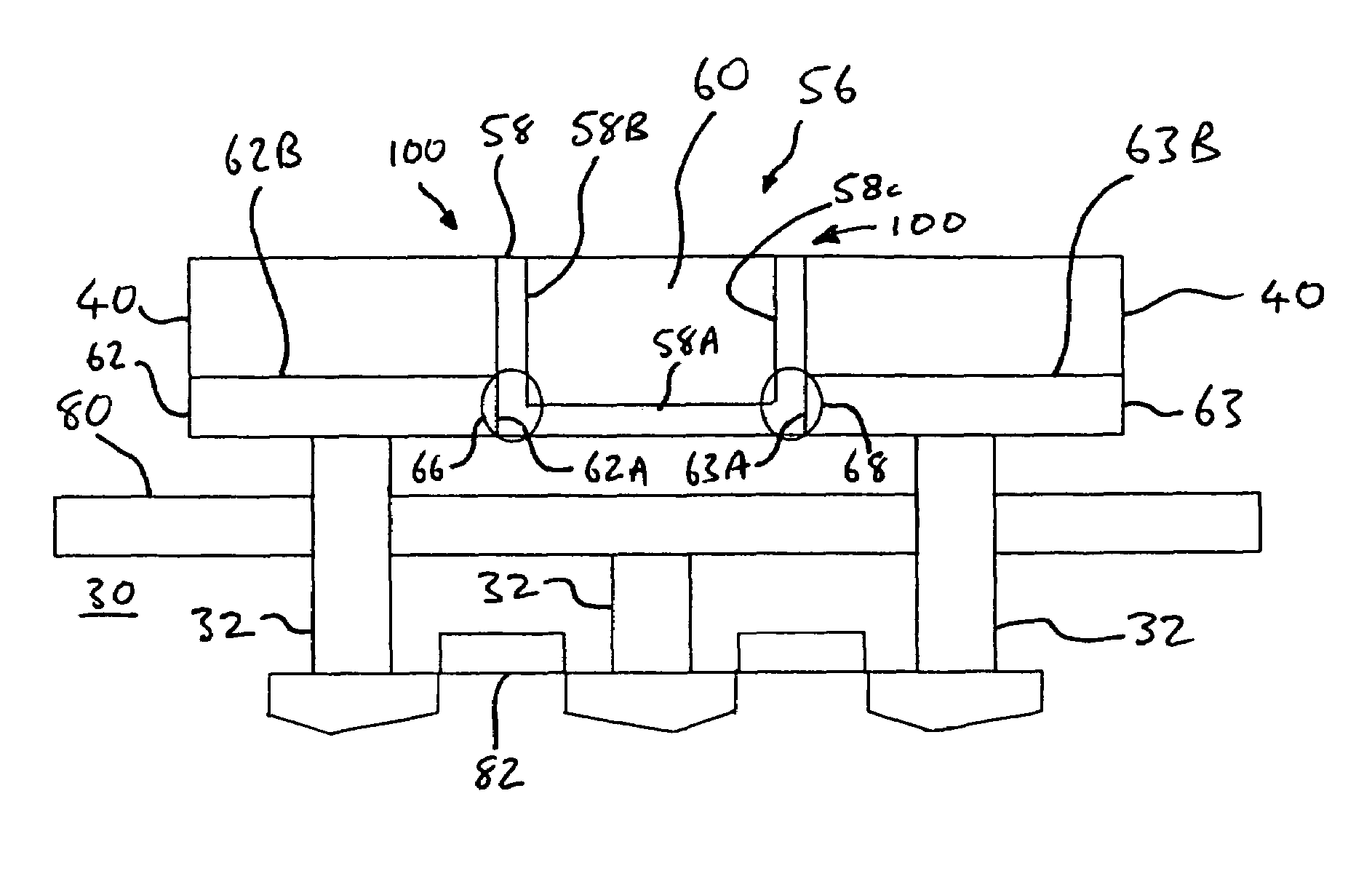
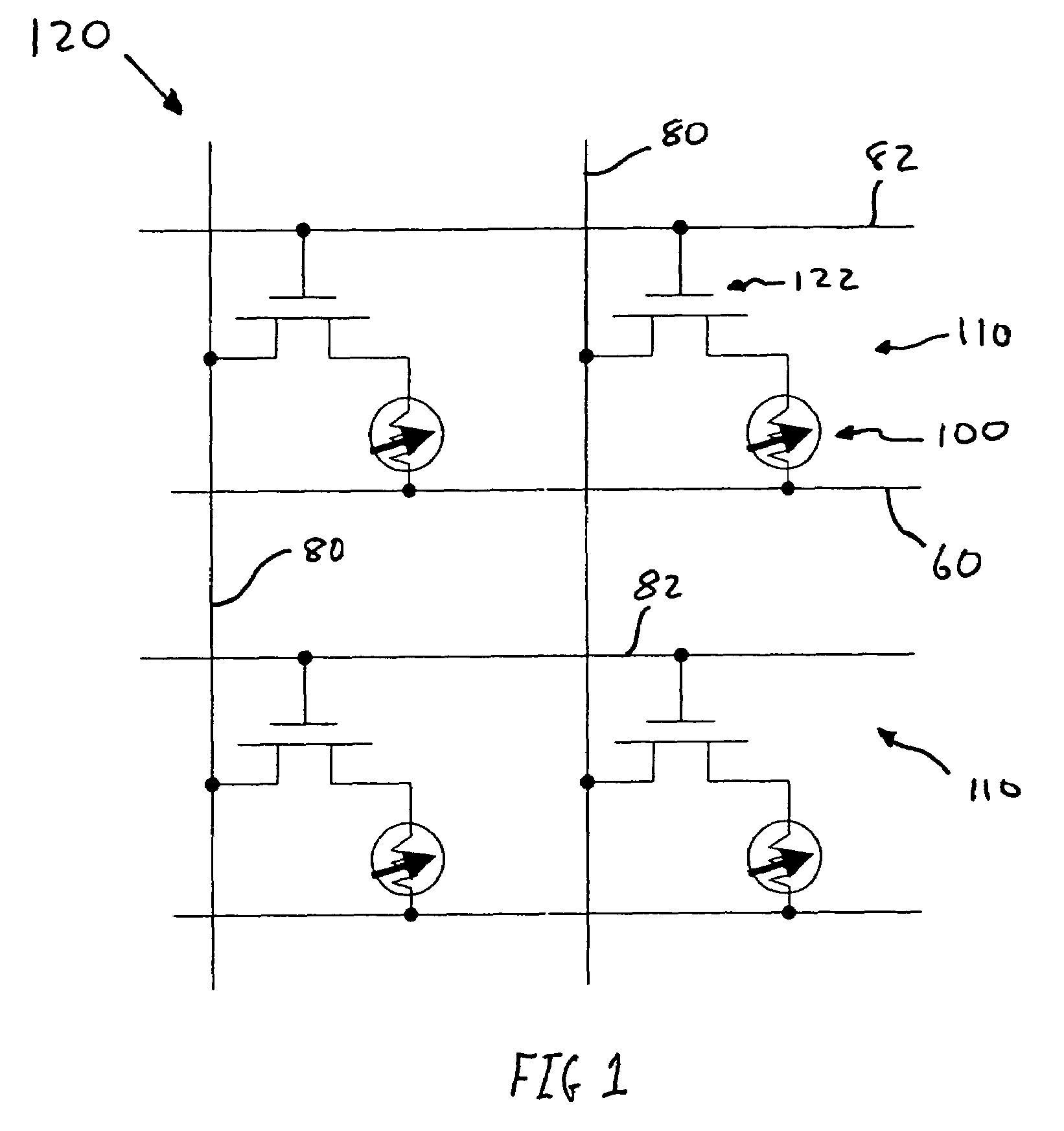
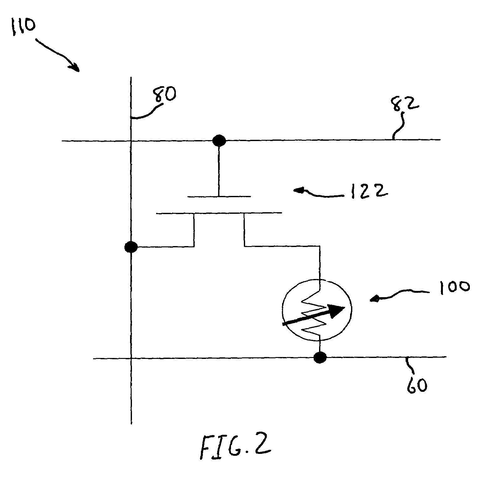
[0043]Reference will now be made in detail to the presently preferred embodiments of the invention, examples of which are illustrated in the accompanying drawings. Wherever possible the same or similar reference numbers are used in the drawings and the description to refer to the same or like parts. It should be noted that the drawings are in simplified form and are not to precise scale. In reference to the disclosure herein for purposes of convenience and clarity only, directional terms, such as top, bottom, left, right, up, down, over, above, below, beneath, rear, front, vertical, horizontal, length, width, and height are used with respect to the accompanying drawings. Such directional terms should not be construed to limit the scope of the invention in any manner.

[0044]Although the disclosure herein refers to certain illustrated embodiments, it is to be understood that these embodiments are presented by way of example and not by way of limitation. The intent of the following deta...


PUM


Abstract

A chalcogenide phase change memory cell has a substrate with a conductor line. The conductor line has a contact end. An insulating layer is located over the substrate and conductor line. An aperture is located in the insulating layer. The aperture extends to the substrate. A memory material is conformally located within the aperture. The memory material is in electrical contact with the contact end. A conductive layer is located over the memory material in the aperture.

Description

BACKGROUND OF THE INVENTION[0001]1. Field of the Invention[0002]The present invention relates generally to memory devices and, more particularly, to a non-volatile chalcogenide memory device.[0003]2. Description of Related Art[0004]Integrated circuits, typically in the form of microprocessors, microcontrollers, or other logic circuits, are used to control the functions of many modern electronic devices. For example, integrated circuits are used to control the functions of computers, telephones, and many other consumer electronics. It is generally necessary for the integrated circuits to retrieve (read) and store (write) data as they perform their functions. The data may be in the form of instructions for the integrated circuits (e.g., a program), data necessary for the execution of a program, or data generated during the execution of the program. It is preferable to store the data in memory devices which are easily accessible by the integrated circuits.[0005]Many different types of ...

Claims


Application Information

Patent Timeline
Patent Type & Authority Patents(United States)
IPC IPC(8): H01L47/00
CPCH01L45/06H01L45/1691H01L45/122H01L45/144H01L27/2436H01L27/2463H10B63/30H10B63/80H10N70/821H10N70/231H10N70/8828H10N70/068
Inventor LUNG, HSIANG-LAN
Owner MACRONIX INT CO LTD
Why Eureka
Try Eureka