Composite motion probing

Inactive Publication Date: 2007-04-10
FORMFACTOR INC
View PDF11 Cites 55 Cited by
  • Summary
  • Abstract
  • Description
  • Claims
  • Application Information

AI Technical Summary

Benefits of technology

[0010]This invention relates generally to probing an electronic device and is particularly applicable to probing a semiconductor device to test the device. An electronic device is moved into a first position with respect to probes for making electrical contact with the device. The electronic device is then moved into a second position in which the electronic device is pressed against the probes, compressing the p

Problems solved by technology

Such forces and stresses may break, damage, or reduce the useful life of a probe 108.
A wafer comprising material with a low “k” dielectric may be particularly susceptible to such damage.
If the probe 108 tip

Method used


Image

  • Composite motion probing
  • Composite motion probing
  • Composite motion probing

Examples


Example

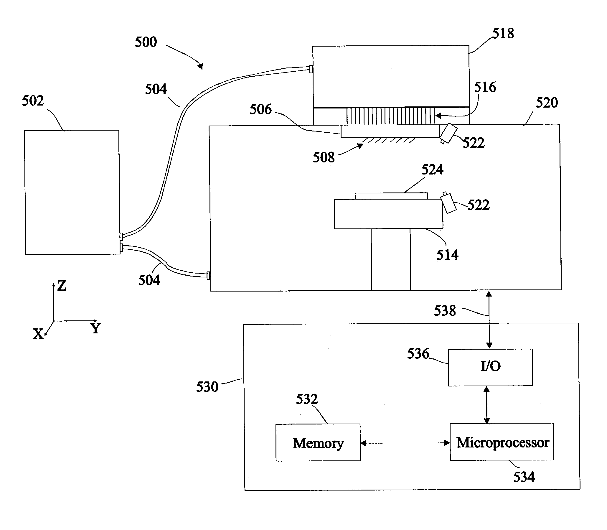
[0028]The present invention relates to probing an electronic device. This specification describes exemplary embodiments and applications of the invention. The invention, however, is not limited to these exemplary embodiments and applications or to the manner in which the exemplary embodiments and applications operate or are described herein.

[0029]FIG. 4 illustrates an exemplary semiconductor test system 500. Test system 500 is exemplary only; other systems in which any type of probe is brought into contact with another device may be used. Nonexclusive examples of such systems include sockets for testing packaged or unpackaged semiconductor devices, or any type of test system in which a semiconductor device (packaged or unpackaged, singulated or unsingulated) is probed. Of course, even if a semiconductor wafer test system is used, a semiconductor test system that is different than the exemplary test system 500 shown in FIG. 4 may be used.

[0030]The exemplary semiconductor test system ...


PUM


Abstract

An electronic device is moved into a first position with respect to probes for making electrical contact with the device. The electronic device is then moved into a second position in which the electronic device is pressed against the probes, compressing the probes. The movement into the second position includes two components. One component of the movement tends to press the electronic device against the probes, compressing the probes and inducing a stress in the probes. The second movement tends to reduce that stress. Test data are then communicated to and from the electronic device through the probes.

Description

FIELD OF THE INVENTION[0001]This invention relates generally to probing an electronic device.BACKGROUND OF THE INVENTION[0002]Although the present invention is generally applicable to probing any electronic device, the present invention is particularly suited for probing an integrated circuit to test the circuit. As is known, integrated circuits are typically manufactured as a plurality of dice on a semiconductor wafer. FIG. 1 illustrates a typical test system 100 for testing such a semiconductor wafer 124. The exemplary test system shown in FIG. 1, includes a tester 102, a test head 118, a probe card 106, and a prober 120.[0003]A semiconductor wafer 124 is placed on a chuck (also commonly referred to as a stage) 114, which typically is capable of movement in the “x,”“y,” and “z” directions. The chuck 114 may also be capable of being rotated and tilted and may be further capable of other motions as well. Once the semiconductor wafer 124 is placed on the chuck 114, the chuck is typic...

Claims


Application Information

Patent Timeline
IPC IPC(8): G01R31/02G01R1/067G01R31/28
CPCG01R31/2887G01R1/06705G01R31/2886
Inventor COOPER, TIMOTHY E.ELDRIDGE, BENJAMIN N.KHANDROS, IGOR Y.MARTENS, RODMATHIEU, GAETAN L.
Owner FORMFACTOR INC
Why Eureka
Try Eureka