Semiconductor device having universal logic cell

a technology of logic cell and semiconductor device, which is applied in the direction of logic circuits characterised by logic functions, logic circuits using specific components, pulse techniques, etc., can solve the problem of limited output driving capability of universal logic modules, and achieve the effects of increasing the switching speed and operation speed of an integrated circuit, enhancing output driving capability, and improving output driving capability

Active Publication Date: 2007-04-17
RENESAS ELECTRONICS CORP
View PDF4 Cites 0 Cited by
  • Summary
  • Abstract
  • Description
  • Claims
  • Application Information

AI Technical Summary

Benefits of technology

[0031]It is an object of the present invention to provide a semiconductor device and a method of manufacturing the same which can enhance the output driving capability and hence increase the switching speed.
[0032]It is another object of the present invention to provide a semiconductor device and a method of manufacturing the same which can prevent the electrostatic destruction and reduce the leak current.
[0033]It is still another object of the present invention to provide a semiconductor device and a method of manufacturing the same which can improve the reliability.
[0045]According to the semiconductor device of present invention, a universal logic module of two input inversion type is used, in which the inverters are provided in the first stage, the transfer gates are provided in the second stage, and middle nodes are exposed on the base layer and can be connected by using interconnections formed in the customize layer. A predetermined node is clamped according to a logic gate to be formed. As a result, it is possible to improve (enhance) the output driving capability and hence to increase the switching speed and the operation speed of an integrated circuit.
[0046]Also, according to the present invention, the source electrodes or the drain electrodes of the N-channel transistor and the P-channel transistor in the transfer gate may be separated and disconnected. Therefore, even if some middle nodes are clamped so as to enhance the output driving capability, the power supply potential is not directly applied to the side of the N-channel transistor of the transfer gate. Thus, the transistor destruction caused by the electrostatic destruction can be prevented, and the leak current can be reduced. It is therefore possible to improve the reliability of the semiconductor device.

Problems solved by technology

According to the conventional technique, as described above, since the input of the inverter is connected to the power supply or the ground, the output driving capability of the universal logic module is limited due to the ON resistance of the P-channel transistor or the N-channel transistor in the inverter.

Method used


Image

  • Semiconductor device having universal logic cell
  • Semiconductor device having universal logic cell
  • Semiconductor device having universal logic cell

Examples


first embodiment

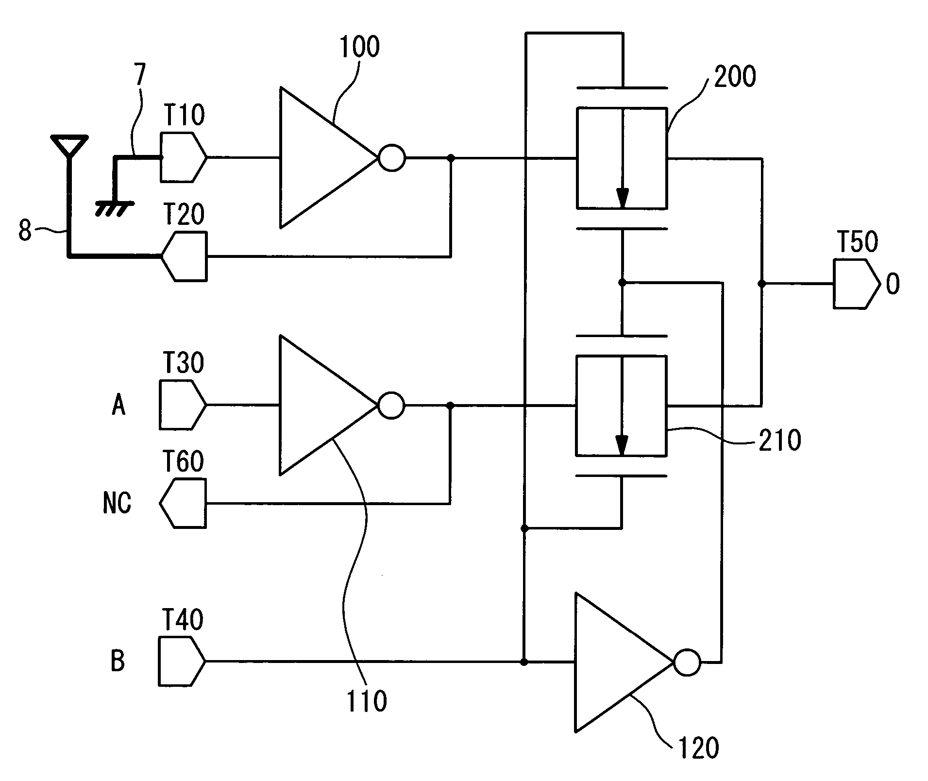
[0086]According to a first embodiment of the present invention, a “NAND” circuit is provided by using the universal logic module. FIG. 6A is a circuit diagram showing a configuration of the NAND circuit achieved by using the universal logic module shown in FIG. 5 according to the present embodiment.

[0087]In the present embodiment, the inverter 100 is used as the “first inverter”, and the transfer gate 200 is used as the “first transfer gate”. Thus, the above-mentioned first input terminal is connected to the first node T10, and the input of the first transfer gate 200 is connected to the second node T20. On the other hand, the inverter 110 is used as the “second inverter”, and the transfer gate 210 is used as the “second transfer gate”.

[0088]As shown in FIG. 6A, the first node T10 of the universal logic module shown in FIG. 5 is connected to the first input terminal, and is connected to an L level (logic “0”), and the second node T20 is connected to an H level (logic “1”). The sixth...

second embodiment

[0091]In a second embodiment of the present invention, a “NAND” circuit is also provided by using a universal logic module.

[0092]FIG. 7 is a circuit diagram showing a configuration of the universal logic module according to the second embodiment of the present invention. Though a basic configuration and a basic operation of the universal logic module in the present embodiment are similar to those in the first embodiment, the output terminals of the inverters, and the input terminals of the transfer gates are different from those in the first embodiment, as described below.

[0093]According to the present embodiment, as shown in FIG. 7, an inverter 100A is formed to have separate outputs; an output from a drain of the Nch transistor and an output from a drain of the Pch transistor. Also, an inverter 110A is formed to have separate outputs; an output from a drain electrode of the Nch transistor and an output from a drain electrode of the Pch transistor. A transfer gate 200A is formed to...

third embodiment

[0103]In a third embodiment of the present invention, a “NAND” circuit is also provided by using a universal logic module.

[0104]FIG. 9 is a circuit diagram showing a configuration of the universal logic module according to the third embodiment of the present invention. Though a basic configuration and a basic operation of the universal logic module in the present embodiment are similar to those in the first embodiment, the input terminals of the transfer gates are different from those in the first embodiment, as described below.

[0105]According to the present embodiment, as shown in FIG. 9, a transfer gate 200B is formed to have separate inputs; an input from a source / drain of the Pch transistor and an input from a source / drain of the Nch transistor. Also, a transfer gate 210B is formed to have separate inputs; an input from a source / drain of the Pch transistor and an input from a source / drain of the Nch transistor.

[0106]More specifically, the universal logic module of the present em...


PUM


Abstract

A universal logic module includes: a first inverter outputting an inverted input signal to an output terminal through a first transfer gate, the inverted input signal having an inverted level of an input signal provided from a first input terminal; and a second inverter outputting an inverted logic signal to the output terminal through a second transfer gate, the inverted logic signal having an inverted level of a first logic signal. The first input terminal is connected to one of a power supply line and a ground line. An input of the first transfer gate is directly connected to the other of the power supply line and the ground line. The first and the second transfer gates are complementarily turned on / off according to a level of a second logic signal. A result of a logical operation between the first and the second logic signals is outputted from the output terminal.

Description

BACKGROUND OF THE INVENTION [0001]1. Field of the Invention[0002]The present invention relates to a semiconductor device. More particularly, the present invention relates to a semiconductor device provided with a universal logic cell (ULC), and a method of manufacturing the semiconductor device.[0003]2. Description of the Related Art[0004]A semiconductor device using a universal logic cell (ULC) and capable of switching at a high speed has been developed.[0005]A “semi-custom technique” is known as a method of designing and manufacturing a semiconductor device by using a universal logic cell and a universal logic module. The semi-custom technique includes a “master slice method”.[0006]According to the master slice method, for example, a universal logic module is formed beforehand in a master slice (base layer), which is known as a structured ASIC (Application Specific Integrated Circuit). The universal logic module is configured to be able to provide a logic gate such as a NAND circu...

Claims


Application Information

Patent Timeline
Patent Type & Authority Patents(United States)
IPC IPC(8): H03K19/20H01L21/822H01L27/04H03K19/173
CPCH03K19/173
Inventor MIZUNO, MASAHARUNAKAJIMA, KAZUHIRO
Owner RENESAS ELECTRONICS CORP
Why Eureka
Try Eureka