Balun device
a transformer and balun technology, applied in the field of balun, can solve the problems of unsuitable devices expected to be built, filter or balun tends to become larger in size, and is difficult to make the band broader, and achieve the effect of miniaturizing the siz
- Summary
- Abstract
- Description
- Claims
- Application Information
AI Technical Summary
Benefits of technology
Problems solved by technology
Method used
Image
Examples
example 1
[0045]Now, Example 1 of balun according to one embodiment of the present invention will be described below referring to FIGS. 1–5.
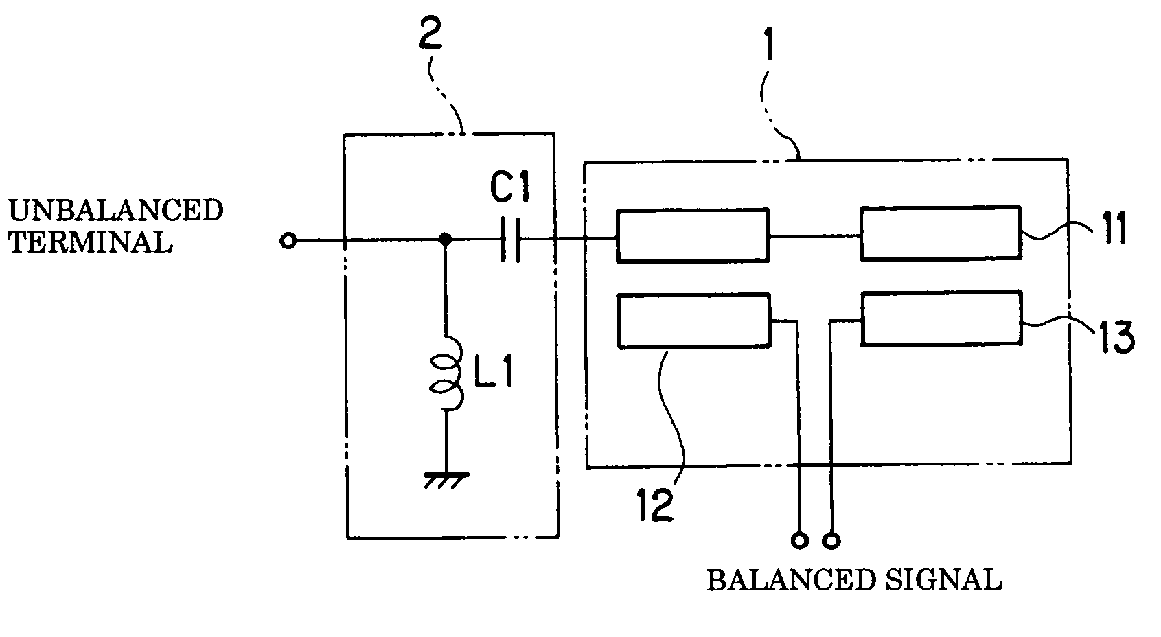
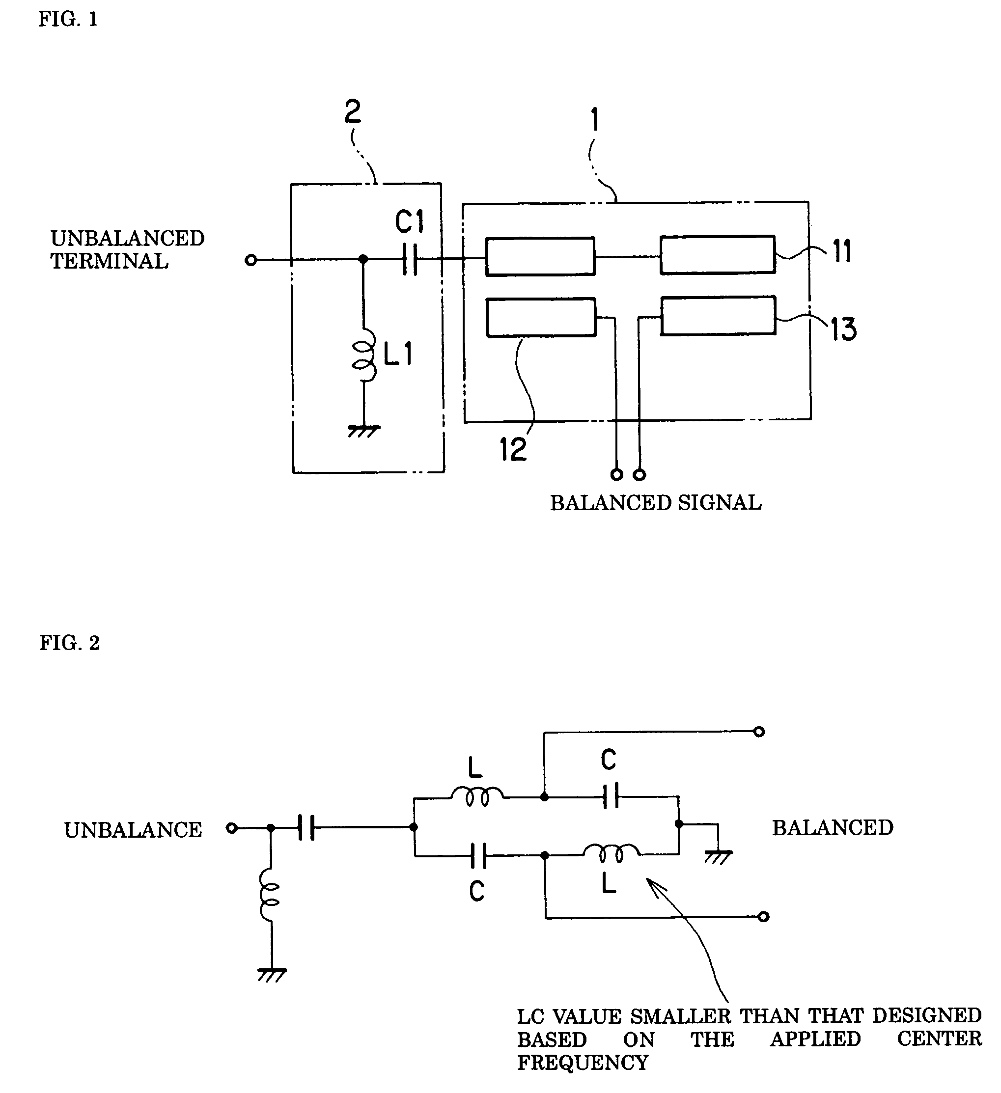
[0046]FIG. 1 is a circuit diagram of the balun showing Example 1, in which the unit numbered 1 shows a balun unit having an unbalanced line 11 and two balanced lines 12, 13, and the unit numbered 2 shows a matching circuit in the form of a high-pass filter, which is composed of a capacitor C1 connected to the unbalanced line and an inductor L1, the capacitor C1 in the matching circuit 2 being connected in series to the unbalanced line 11 and the inductor L1 being connected in parallel to the unbalanced line 11 through the capacitor C1.
[0047]When the balun unit 1 is composed of strip lines, the length of a strip line in the balun unit is made shorter than λ / 4 of the applied center frequency (the center frequency defined in the communications standard), while, when the balun unit 1 is composed of an LC element the LC circuit is configured so as to give a sm...
example 2
[0051]In Example 2, the matching circuit 2 is composed of two capacitors C1, C2, which are connected in series to the unbalanced line 11 as shown in FIG. 6, and an inductor L1 which is connected to the joining point between the two capacitors C1, C2, and it provides the improved ultra wide band characteristic that is nearly the same as in the above-described Example 1 (See FIG. 7).
[0052]Here, in the figure, dotted line indicates the property without the matching circuit 2; and solid line indicates the property with the matching circuit 2 connected. The same indication will be used hereinafter.
example 3
[0053]In Example 3, the matching circuit 2 is composed of a capacitor C1 which is connected in series to the unbalanced line 11 as shown in FIG. 8, and two inductors L1, L2 which are connected to both ends of the capacitor C1. Although the result shows an abnormal waveform partially at lower frequency, its ultra wide band is still secured (See FIG. 9).
PUM
 Abstract
Description
Claims
Application Information


