Package substrate manufactured using electrolytic leadless plating process, and method for manufacturing the same

a leadless plating and packaging substrate technology, applied in the field of packaging substrates, can solve the problems of pins or leads may be easily broken, and the pins or leads are difficult to achieve high-density integration of au-plating lead lines, so as to avoid noise generation, improve the line density of the package substrate, and eliminate the effect of plating lead lines

Inactive Publication Date: 2007-04-24
SAMSUNG ELECTRO MECHANICS CO LTD
View PDF12 Cites 5 Cited by
  • Summary
  • Abstract
  • Description
  • Claims
  • Application Information

AI Technical Summary

Benefits of technology

[0021]The present invention has been made in view of the above mentioned problems, and an object of the invention is to provide a package substrate manufactured in a semi-additive manner without using any plating lead line, thereby being capable of achieving an improvement in line density, and a method for manufacturing the package substrate.
[0022]Another object of the invention is to provide a package substrate capable of completely removing all plating lead lines used in a normal electrolytic Au plating process, thereby achieving suppression of noise.
[0031]In accordance with the present invention, it is possible to manufacture a package substrate without using any plating lead line because an Au layer is plated on wire bonding pads and solder ball pads in a semi-additive manner without using any plating lead line in accordance with an electrolytic Au plating process. Accordingly, it is possible to achieve an improvement in the line density of the package substrate, while avoiding generation of noise by virtue of elimination of plating lead lines.

Problems solved by technology

Although such a PGA carrier can have a number of leads while having a miniature size, it has a drawback in that its pins or-leads may be easily broken due to their low strength, or involves a limitation of high-density integration.
Substantially, there is a limitation of high-density integration in designing a circuit, due to such plating lead lines.
However, the above mentioned conventional BGA package substrate 10 involves a problem in that it is difficult to achieve high-density integration of the Au-plating lead lines adapted to carry out an Au plating process for the bond fingers 1 and pads 7 because the pitch of the solder balls 8 in the BGA package substrate, that is, the space between adjacent solder balls, is rendered to be very small due to high-density integration of circuits and miniaturization of devices using such circuits, and because of high-density integration of circuits arranged around the bond fingers 1 of the outer-layer circuit mounted with the semiconductor chip thereon.
Such a reduced line density causes a problem in manufacturing a circuit having a high-density integration.
However, the plating lead lines are incompletely removed from the package substrate.
The residues of the plating lead lines may cause noise during transmission of electrical signals in the circuits provided at the package substrate.
As a result, there is a degradation in electrical performance.
In the case of the solder ball pads, however, such a thickness is excessive, as compared to an appropriate thickness of 0.03 to 0.25 μm.
For this reason, there is a problem associated with the reliability of the bonding of solder balls.

Method used


Image

  • Package substrate manufactured using electrolytic leadless plating process, and method for manufacturing the same
  • Package substrate manufactured using electrolytic leadless plating process, and method for manufacturing the same
  • Package substrate manufactured using electrolytic leadless plating process, and method for manufacturing the same

Examples


Embodiment Construction

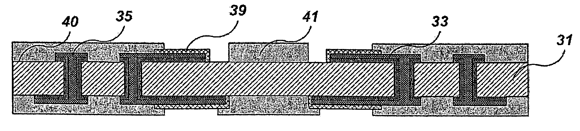
[0044]Now, a package substrate manufactured using an electrolytic leadless plating process without using any plating lead line and a method for manufacturing the same in accordance with each embodiment of the present invention will be described in detail.

[0045]FIGS. 6a to 6k are views illustrating processes for manufacturing a package substrate in a semi-additive manner without using any plating lead line in accordance with an embodiment of the present invention, respectively. The package substrate and its manufacturing method will be described in conjunction with FIGS. 6a to 6k.

[0046]First, a plurality of through holes, that is, via holes, 32, are formed at a base substrate 31 (FIG. 6a). A first copper plated layer 33 is formed to cover the entire surface of the base substrate 31 and the inner surface of each through hole 32 (FIG. 6b). The plating of the first copper plated layer 33 is carried out in accordance with an electroless plating process. The first copper plated layer 33 ...


PUM

PropertyMeasurementUnit
thicknessaaaaaaaaaa
thicknessaaaaaaaaaa
thicknessaaaaaaaaaa

Abstract

A method of manufacturing a package substrate includes forming a first copper plated layer on a base substrate having through holes and inner surfaces of the through hole, coating a first resist over the first copper plated layer, partially removing the first resist, forming a second copper plated layer on the first copper plated layer, stripping the first resist, coating a second resist over the resultant structure, and removing the second resist from regions where wire bonding pads and solder ball pads are to be formed, removing exposed portions of the first copper plated layer, forming the wire bonding pads and the solder ball pads, removing the second resist, removing exposed portions of the first copper plated layer, and coating a solder resist over all surfaces of the resultant structure, and removing portions of the solder resist respectively covering the wire bonding pads and the solder ball pads.

Description

[0001]This is a divisional application of copending Application Ser. No. 10 / 609,499 filed on July 1, 2003.BACKGROUND OF THE INVENTION[0002]1. Field of the Invention[0003]The present invention relates to a package substrate manufactured using an electrolytic leadless plating process, and a method for manufacturing the same. More particularly, the present invention relates to a package substrate of, for example, a ball grid array (BGA) type or a chip scale package (CSP) type, manufactured by electrolytically plating Au in a semi-additive manner without using any plating lead line on wire bonding pads to be connected with a semiconductor chip mounted on a base substrate, and solder ball pads, and a method for manufacturing the same.[0004]2. Description of the Related Art[0005]In-spite of the recent tendency of integrated circuits to have a light, thin, simple and miniature structure, integrated circuit packages rather tend to have an increased number of leads extending outwardly theref...

Claims


Application Information

Patent Timeline
Patent Type & Authority Patents(United States)
IPC IPC(8): H01L21/44C25D7/12C25D5/02C25D5/10H01L21/48H01L23/12H01L23/28H05K3/10H05K3/24H05K3/42
CPCH01L21/4846H05K3/243H01L21/4857H01L2924/01019H01L2224/32225H01L2224/48091H01L2224/48227H01L2224/73265H01L2924/01078H01L2924/01079H01L2924/15311H05K3/108H05K3/426H05K2203/1476Y10T29/49155H01L2924/00014H01L2924/00H01L2924/00012H01L24/73H01L2924/14H01L23/28
Inventor LEE, JONG-JINSHIN, YOUNG-HWAN
Owner SAMSUNG ELECTRO MECHANICS CO LTD
Why Eureka
Try Eureka