Semiconductor device

a technology of semiconductor devices and semiconductors, applied in semiconductor devices, semiconductor/solid-state device details, electrical apparatus, etc., can solve the problems of affecting the reliability of semiconductor devices, and increasing manufacturing costs, so as to reduce reliability and increase manufacturing costs

Inactive Publication Date: 2007-04-24
RENESAS ELECTRONICS CORP
View PDF8 Cites 11 Cited by
  • Summary
  • Abstract
  • Description
  • Claims
  • Application Information

AI Technical Summary

Benefits of technology

[0011](1) The package structure, wherein leads are exposed from the back side of a resin sealing member to form external terminals, is obtained by positioning a lead frame within a molding die so that the leads come into contact with an inner surface of a cavity of a molding die, and, thereafter, resin is injected into the cavity of the molding die. However, the front end portions of the leads are not supported anywhere and are free, so that the leads are apt to be displaced by the flow of resin injected into the cavity. Since this lead displacement during molding causes the adhesion between t

Problems solved by technology

However, the front end portions of the leads are not supported anywhere and are free, so that the leads are apt to be displaced by the flow of resin injected into the cavity.
Since this lead displacement during molding causes the adhesion between the cavity and the leads to be deteriorated, there easily occurs an inconvenience in that the exposed portions of the leads serving as back electrodes (external terminals) of the resin sealing member are covered with resin flash.
This inconvenience based on the presence of resin flash lowers the reliability at the time of soldering the semiconductor device onto a wiring substrate.
In addition, a process for removing the resin flash is needed, thus resulting in an increase in the manufacturing cost.
As a result, however, the external terminals are also microsized.
The external terminals are required to h

Method used


Image

  • Semiconductor device
  • Semiconductor device
  • Semiconductor device

Examples


first embodiment

[0116]In connection with this first embodiment, the description will be directed to an example in which the present invention is applied to a QFN type semiconductor device.

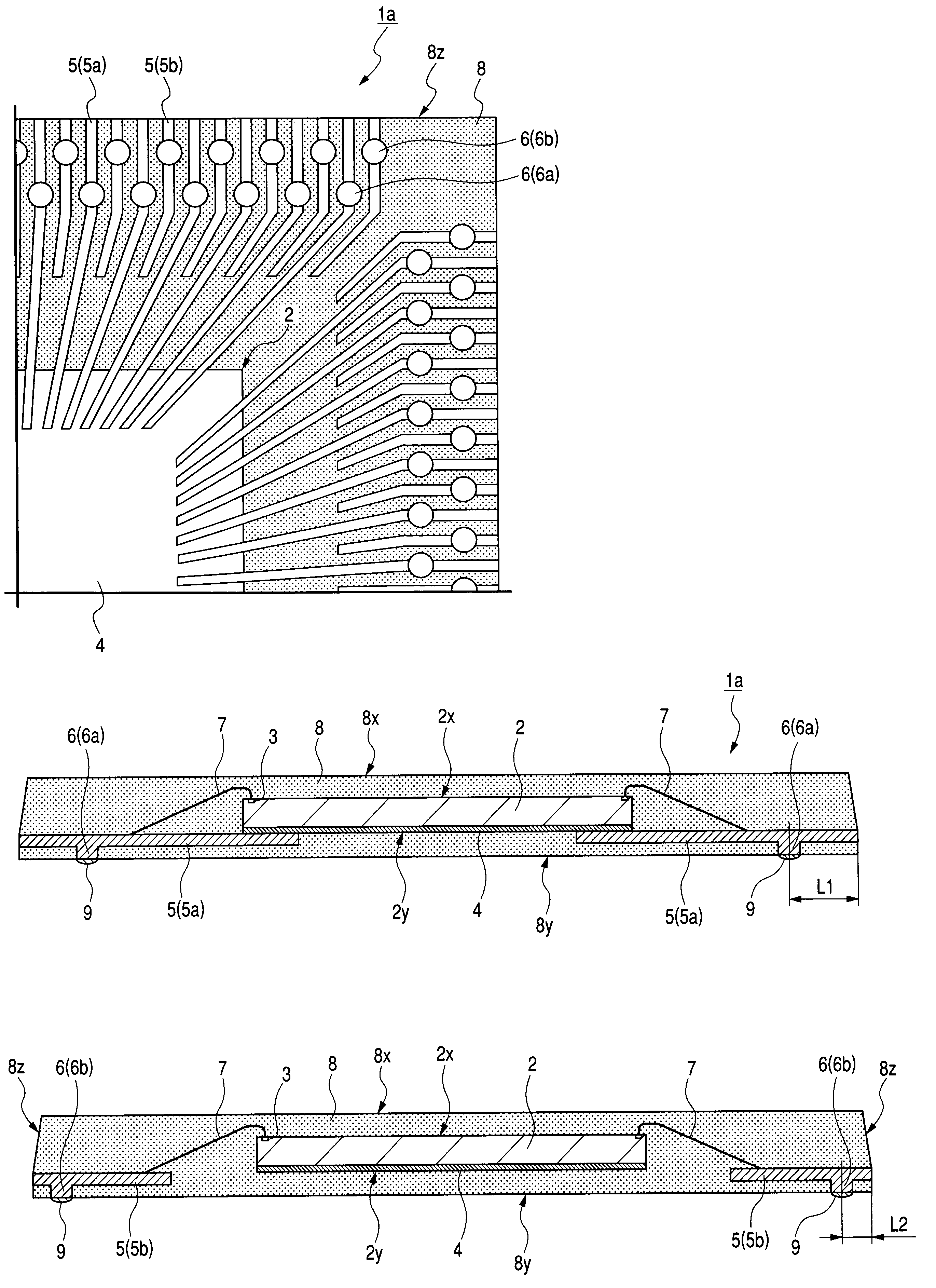
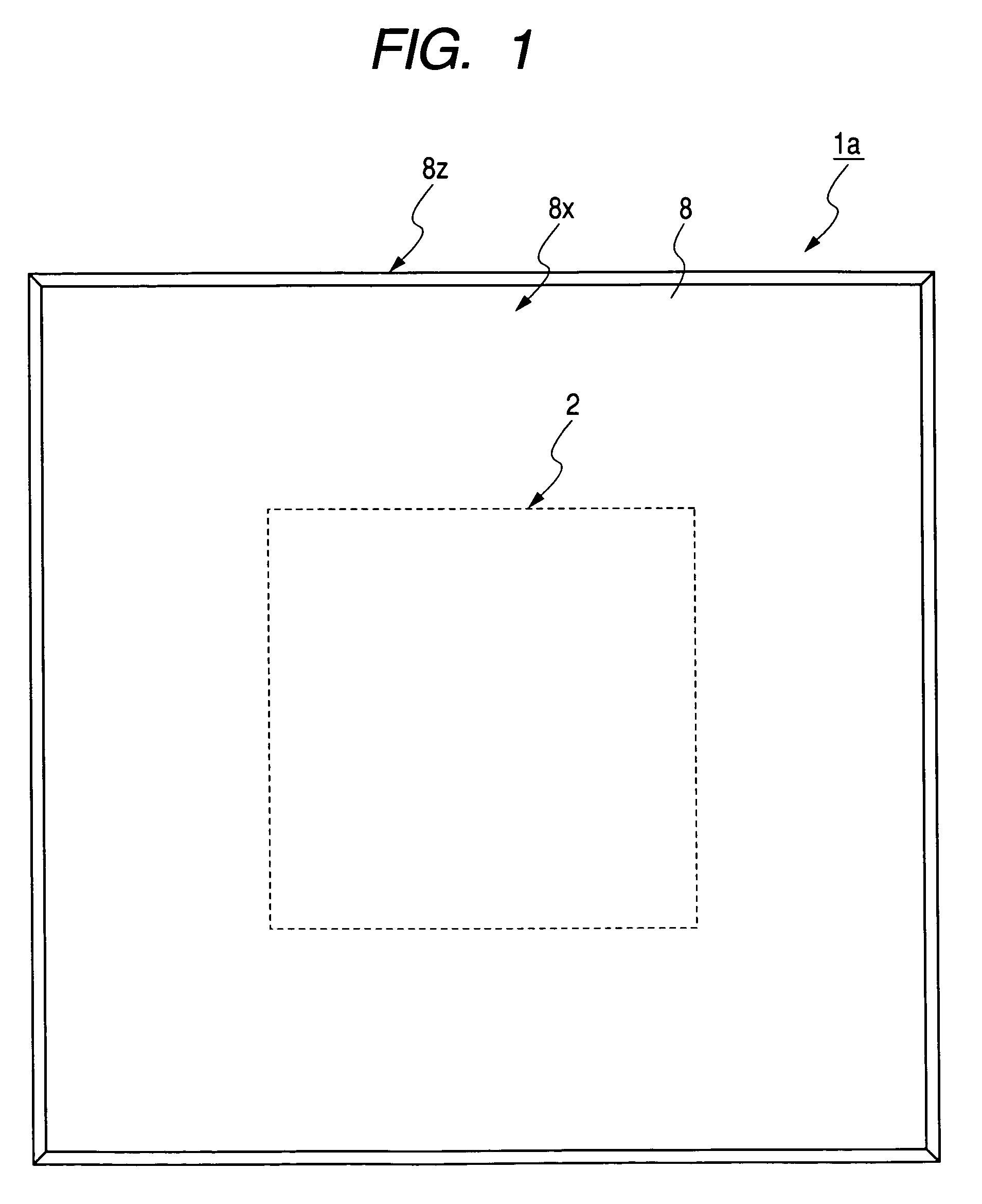
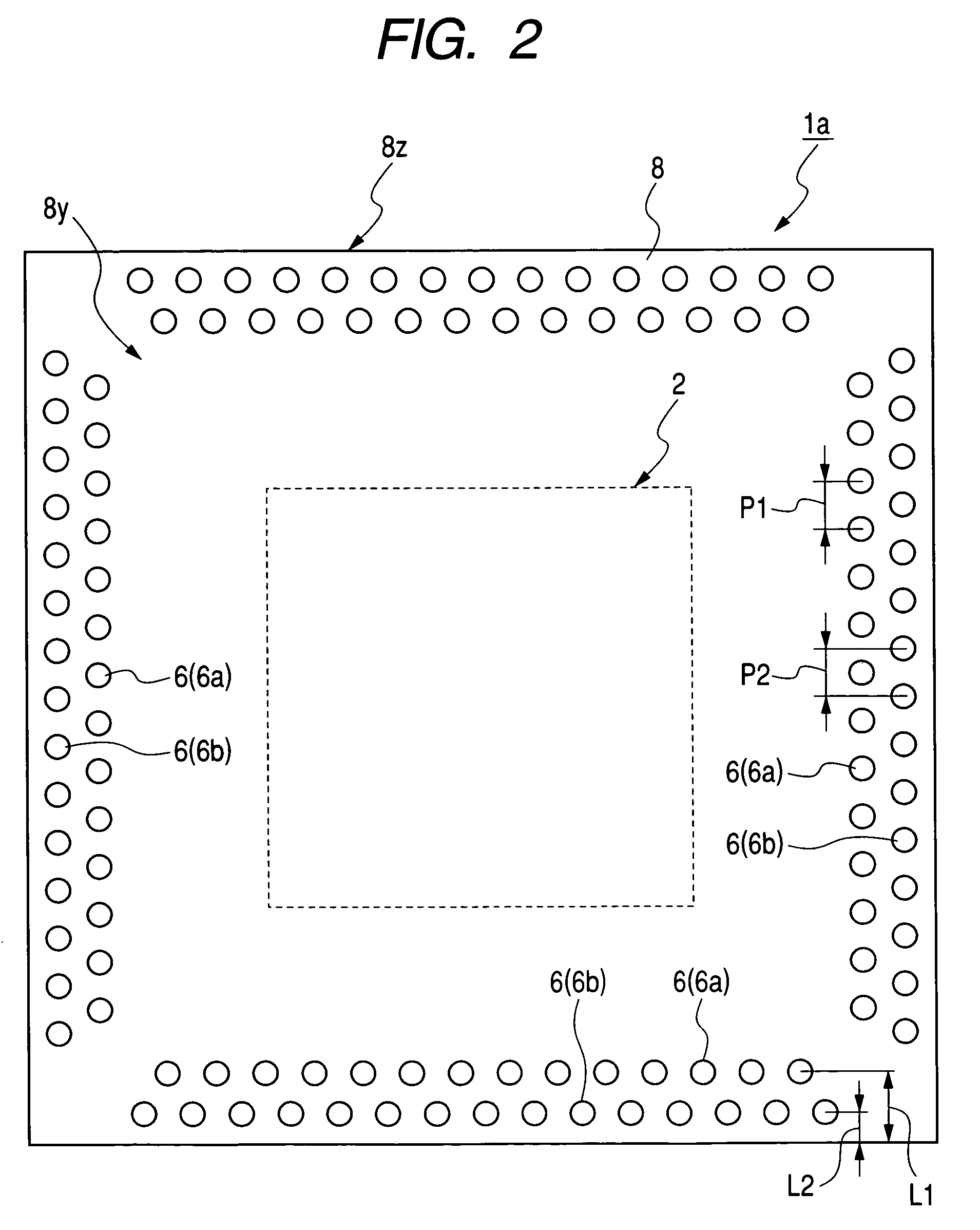
[0117]FIG. 1 is a plan view (top view) showing the appearance of a semiconductor device according to the first embodiment of the present invention; FIG. 2 is a bottom view (underside view) showing the appearance of the semiconductor device; FIG. 3 is a plan view (top view) showing an internal structure of the semiconductor device; FIG. 4 is a plan view corresponding to a partially enlarged view of FIG. 3; FIG. 5 is a bottom view (underside view) showing an internal structure of the semiconductor device; FIG. 6 is a bottom view corresponding to a partially enlarged view of FIG. 5; FIG. 7A is a sectional view taken along line a—a (first leads) in FIG. 3; and FIG. 7B is a sectional view taken along line b—b in FIG. 3.

[0118]In FIGS. 3 and 4, wires which will be described later are partially omitted to make the drawing...

second embodiment

[0166]FIGS. 18A and 18B are sectional views showing an internal structure of a semiconductor device according to a second embodiment of the present invention, of which FIG. 18A is a sectional view taken along first leads and FIG. 18B is a sectional view taken along second leads.

[0167]As shown in FIGS. 18A, 18B, a semiconductor device 1b of this second embodiment basically has the same configuration as the first embodiment and is different in the following configuration.

[0168]The semiconductor device 1b of this second embodiment has a package structure wherein the semiconductor device has a base (support base) 10 for supporting the semiconductor chip 2, the semiconductor chip 2 being bonded and fixed to a main surface of the base 10 through the adhesive 4, and end portions on one side of leads 5 (5a, 5b) are bonded and fixed through an adhesive to a back side of the base 10 opposite to the main surface. As the base 10, it is preferable to use an insulating base, such as a resin tape,...

third embodiment

[0171]FIGS. 19A and 19B are sectional views showing an internal structure of a semiconductor device according to a third embodiment of the present invention, of which FIG. 19A is a sectional view taken along first leads and FIG. 19B is a sectional view taken along second leads.

[0172]As shown in FIGS. 19A, 19B, a semiconductor device 1c of this third embodiment basically has the same configuration as the second embodiment and is different in the following configuration.

[0173]The semiconductor device 1c of this third embodiment has a package structure wherein end portions on one side of leads 5 (5a, 5b) are bonded and fixed to the main surface (the surface to which the semiconductor chip 2 is fixed, i.e., the chip-fixed surface) of the base 10 at positions around (outside) the semiconductor chip 2. The leads 5 each have a first portion S1, a second portion S2 bent from the first portion S1 to the back surface 8y of the resin sealing member 8, and a third portion S3 extending from the ...


PUM


Abstract

A semiconductor device has an, improved mounting reliability and has external terminals formed by exposing portions of leads from a back surface of a resin sealing member. End portions on one side of the leads are fixed to a back surface of a semiconductor chip, and portions of the leads positioned outside the semiconductor chip are connected with electrodes formed on the semiconductor chip through wires.

Description

CLAIM OF PRIORITY[0001]The present application claims priority from Japanese patent application JP 2003-141911, filed on May 20, 2003, the contents of which is hereby incorporated by reference into this application.BACKGROUND OF THE INVENTION[0002]The present invention relates to a semiconductor device. Particularly, the present invention is concerned with a technique that is applicable to a semiconductor device having external terminals formed by exposing leads partially from a back surface (a component side) of a resin sealing member.[0003]As to semiconductor devices wherein a semiconductor chip with an integrated circuit formed thereon is sealed with resin, those of various package structures have been proposed and produced on a commercial basis. As one example, there is a semiconductor device called a QFN (Quad Flatpack Non-Leaded Package) type. This QFN type semiconductor device has a package structure wherein leads connected electrically to electrodes on a semiconductor chip a...

Claims


Application Information

Patent Timeline
IPC IPC(8): H01L23/495H01L23/48H01L23/52H01L29/40H01L23/12H01L21/56H01L21/60H01L23/16H01L23/28H01L23/50
CPCH01L21/565H01L23/16H01L23/49506H01L23/4951H01L23/49548H01L24/27H01L24/29H01L24/97H01L2224/274H01L2224/48091H01L2224/48247H01L2224/49171H01L2224/73265H01L2224/83191H01L2224/92247H01L2224/97H01L2924/01004H01L2924/01013H01L2924/01027H01L2924/01029H01L2924/01033H01L2924/01047H01L2924/0105H01L2924/01057H01L2924/01078H01L2924/01079H01L2924/01082H01L2924/14H01L2924/15311H01L2924/1532H01L24/48H01L24/49H01L2224/29H01L2224/29298H01L2224/32245H01L2924/01005H01L2924/01006H01L2924/014H01L2224/29101H01L2924/0132H01L2224/45144H01L2224/2919H01L2924/00013H01L2924/10253H01L2924/07802H01L2924/00014H01L2224/85H01L2224/83H01L2924/00H01L2924/01026H01L2924/01028H01L2224/29099H01L2224/29199H01L2224/29299H01L2224/2929H01L2924/00012H01L24/45H01L24/73H01L2224/05554H01L2224/16145H01L2224/48257H01L2924/181H01L2924/18161H01L2224/05599H01L23/28H01L23/50H01L21/60
Inventor ITO, FUJIOSUZUKI, HIROMICHI
Owner RENESAS ELECTRONICS CORP
Why Eureka
Try Eureka