Semiconductor device having a particular electrode structure

a technology of a particular electrode structure and a semiconductor device, which is applied in the direction of printed circuit components, conductive pattern reinforcement, printed circuit manufacturing, etc., can solve the problems of reducing affecting the performance of the device, so as to inhibit the reduction of the strength of the connection interface and prolong the life of the thermal fatigu

Inactive Publication Date: 2007-05-01
RENESAS ELECTRONICS CORP
View PDF1 Cites 5 Cited by
  • Summary
  • Abstract
  • Description
  • Claims
  • Application Information

AI Technical Summary

Benefits of technology

[0009]Meanwhile, as the method for solving the problems described above, the inventors of the prevent invention have created the structure in which the solder with a certain thickness is coated in advance on the electrode pad. The structure of this solder coating method is shown in FIG. 15A (the structure of the BGA connection method using solder ball is shown in FIG. 15B for comparison). In this structure, since the amount of solder used for the connection is increased in comparison to the LGA, the occurrence of connection failure due to the warp of the package can be inhibited. Also, since the package / substrate distance is increased, the thermal fatigue life can be extended. Furthermore, since Au and Pd of the metallization of the pad can be dissolved into the solder, it is possible to prevent the Au—Zn compound and Pd—Zn compound from being formed at the connection interface when the Sn—Zn series solder is used for the connection. As a result, it is possible to inhibit the reduction of the strength of the connection interface.
[0010]However, in the structure in which the solder is coated, the coating process is problematic. When using the solder ball or the solder paste printing and the metallization of the pad contains Au and Pd, it is possible to remove Au and Pd from the solder / metallization connection interface by dissolving Au and Pd into the solder. However, since the Au—Sn compound and Pd—Sn compound are collected in the solder adjacent to the connection interface, the strength of the connection interface is reduced, and the interfacial breaking frequently occurs. For its prevention, the dipping method and flow solder method which can remove the compound adjacent to the connection interface are considered as candidates. In these methods, however, since the amount of solder to be coated depends on the pad area, if the fine pitch is employed in the future, it is impossible to supply the amount of solder capable of preventing the occurrence of the connection failure due to the warp of the package and the substrate and providing the desired thermal fatigue life.
[0011]In such a circumstance, an object of the present invention is to provide a technology capable of forming a semiconductor device having an electrode pad coated with solder in which the reduction of the strength of the connection interface can be prevented, the connection failure due to the warp does not occur, and the necessary thermal fatigue life can be provided by performing the solder coating while using the dipping method and the solder paste printing in combination.
[0017]According to the present invention, it is possible to realize a semiconductor device having an electrode pad coated with solder in which the reduction of the strength of the connection interface can be prevented, the connection failure due to the warp does not occur, and the necessary thermal fatigue life can be provided by performing the solder coating while using the dipping method and the solder paste printing in combination.

Problems solved by technology

However, in the structure in which the solder is coated, the coating process is problematic.
However, since the Au—Sn compound and Pd—Sn compound are collected in the solder adjacent to the connection interface, the strength of the connection interface is reduced, and the interfacial breaking frequently occurs.
In these methods, however, since the amount of solder to be coated depends on the pad area, if the fine pitch is employed in the future, it is impossible to supply the amount of solder capable of preventing the occurrence of the connection failure due to the warp of the package and the substrate and providing the desired thermal fatigue life.

Method used


Image

  • Semiconductor device having a particular electrode structure
  • Semiconductor device having a particular electrode structure
  • Semiconductor device having a particular electrode structure

Examples


Embodiment Construction

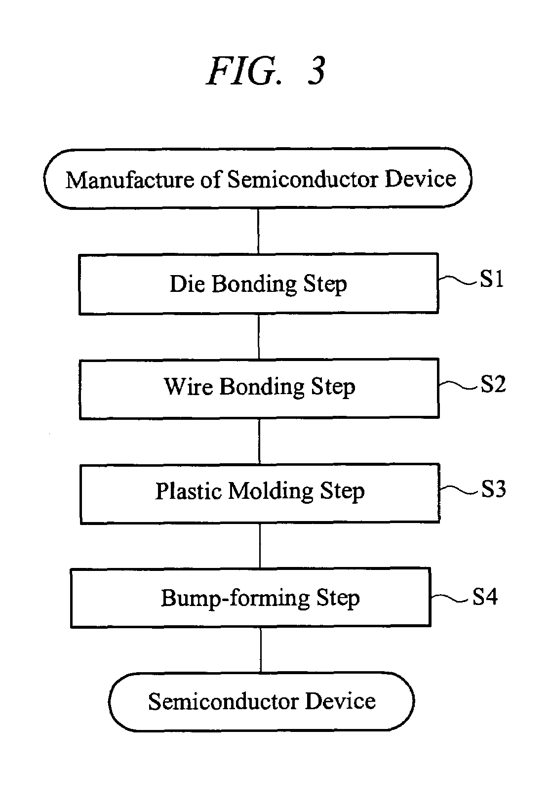
[0033]Hereinafter, embodiments of the present invention will be described in detail with reference to the accompanying drawings. Note that components having the same function are denoted by the same reference symbols throughout the drawings for describing the embodiment, and the repetitive description thereof will be omitted.

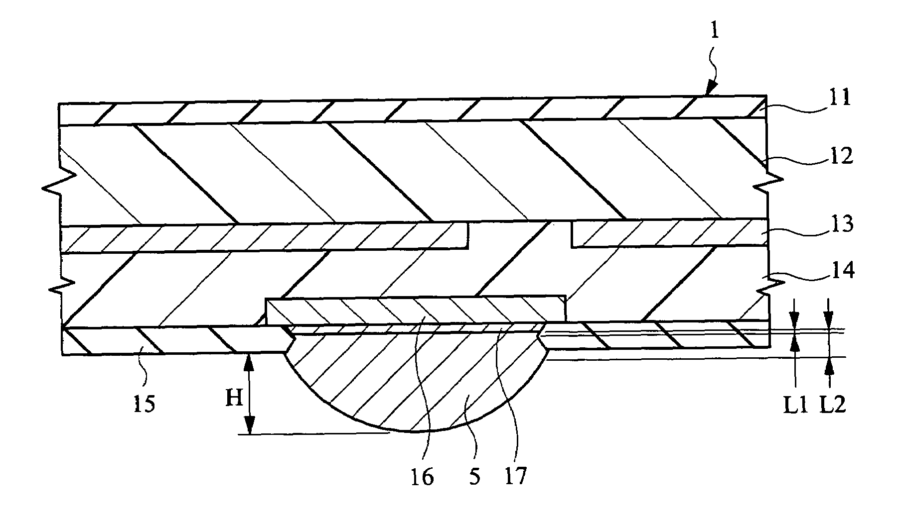
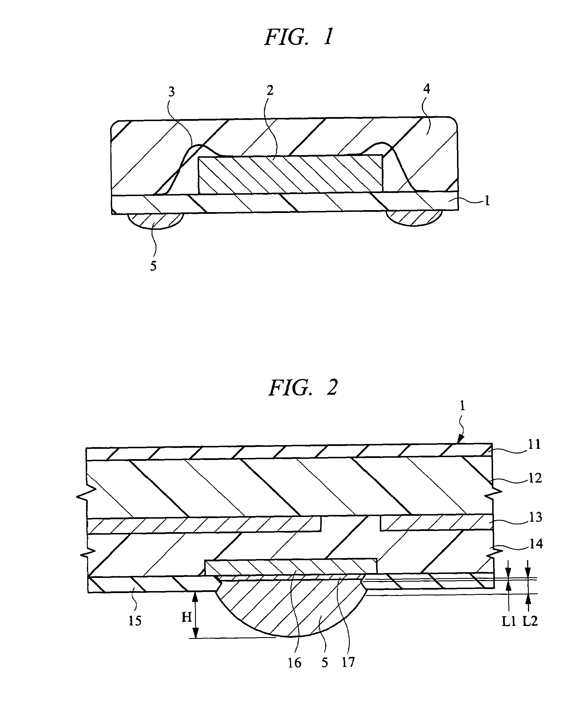
[0034]First, an example of the structure of the semiconductor device according to an embodiment of the present invention will be described with reference to FIGS. 1 and 2. FIG. 1 is a cross-sectional view of the semiconductor device and FIG. 2 is an explanatory diagram of the dimensions of the metal bump, respectively.

[0035]The semiconductor device according to this embodiment comprises a package substrate 1 (described merely as a substrate, hereinafter), a semiconductor chip 2 mounted on the substrate 1, bonding wires 3 which electrically connect the pads on the substrate 1 and the electrodes on the semiconductor chip 2, a molding resin 4 for encapsulating expo...


PUM

PropertyMeasurementUnit
heightaaaaaaaaaa
temperatureaaaaaaaaaa

Abstract

In order to inhibit the connection failure due to the degradation of the connection interface strength of the electrode pad and the warp thereof in the semiconductor device having an electrode pad, a metal layer formed on the electrode pad, and a metal bump formed on the metal layer, in the present invention, gold (Au) is contained in the metal layer, the metal bump is made of solder mainly made of Sn and designed to have an average height H of 100 μm or less per unit area in the electrode pad, and the concentration of Au of the metal layer dissolved in the solder is set to 1.3×10⁻³ (Vol %) or less. More preferably, the metal bump contains palladium (Pd), and the solder coating for forming the metal bump on the electrode pad is performed by using the dipping and the paste printing in combination.

Description

CROSS-REFERENCE TO RELATED APPLICATION[0001]The present application claims priority from Japanese Patent Application No. JP2004-170234 filed on Jun. 8, 2004, the content of which is hereby incorporated by reference into this application.TECHNICAL FIELD OF THE INVENTION[0002]The present invention relates to a semiconductor device and a manufacturing method thereof. More particularly, the present invention relates to a technology effectively applied to a solder-coating method of an electrode pad for realizing a solder connecting portion which does not reduce the connection reliability even in a packaging component which can achieve the reduction in space and thickness and to a packaging component created in accordance with the solder-coating method.BACKGROUND OF THE INVENTION[0003]The miniaturization of mobile devices such as a mobile phone and PDA (Personal Digital Assistant) has been progressing and the performance thereof has been improved more and more in recent years, and the BGA...

Claims


Application Information

Patent Timeline
Patent Type & Authority Patents(United States)
IPC IPC(8): H01L29/40H01L23/12H01L21/60H01L23/498H01L25/10H05K3/06H05K3/24H05K3/34
CPCH01L23/49816H01L24/11H01L24/12H01L25/105H05K3/3463H01L2224/13099H01L2224/16H01L2224/32145H01L2224/48227H01L2924/01013H01L2924/01015H01L2924/01029H01L2924/0103H01L2924/01046H01L2924/01047H01L2924/01078H01L2924/01079H01L2924/01082H01L2924/15153H01L2924/1517H01L2924/15311H01L2924/1532H01L2924/15331H05K3/067H05K3/244H05K2201/0305H05K2203/0361H05K2203/1476H01L24/48H01L2924/01005H01L2924/01006H01L2924/01023H01L2924/01033H01L2924/014H01L2924/3511H01L2225/1035H01L2225/1058H01L2224/11822H01L2924/181H01L2224/05022H01L2224/05026H01L2224/0557H01L2224/05001H01L2224/05147H01L2224/05155H01L2224/05164H01L2224/05644H01L2924/00014H01L2224/05571H01L2924/00012H01L2224/45099H01L2224/45015H01L2924/207
Inventor YAMASHITA, SHIROABE, YOICHIYAMAMOTO, KENICHIKIMOTO, RYOSUKEKAWAKUBO, HIROSHI
Owner RENESAS ELECTRONICS CORP
Why Eureka
Try Eureka