
Electronic components and method of fabricating the same

Active Publication Date: 2007-05-08
STMICROELECTRONICS SRL
View PDF16 Cites 0 Cited by
  • Summary
  • Abstract
  • Description
  • Claims
  • Application Information

AI Technical Summary

Benefits of technology

[0015]In view of these drawbacks, it is an object of the present invention to remove the above-mentioned drawbacks and to compensate for the imprecision in pos

Problems solved by technology

The production of electronic components on the surface of a semiconductor substrate results in general from a complex process which is subject to constraints of various types.
Other constraints, of a geometrical nature, result from the technological trend pertaining to this type of component towards ever higher levels of integration.
This trend necessitates the design of more compact arrangements of components, which cannot be achieved by standard fabrication processes for integrated circuits.
Yet other constraints may be of a mechanical nature, associated with the deformation liable to occur when the components are heated.
However, certain materials incorporated into upper levels may have to be subjected in situ to heat treatments at high temperature, whereas materials incorporated into lower levels would be degraded by such heat treatments.
One drawback of these types of methods which proceed by transferring an initial structure between two substrates appears during the continuation of the production of the structure on top of the initial structure portion that is transferred.
However, this mask positioning step is complex and often requires several adjustments in order to obtain sufficient alignment precision.
Furthermore, the high levels of integration currently sought, corresponding for example to 0.12 micron or 0.10 micron technologies, or yet even finer technologies, appear to be incompatible with an intervening positioning step while certain of the components are only partly produced.

Method used


Image

  • Electronic components and method of fabricating the same
  • Electronic components and method of fabricating the same
  • Electronic components and method of fabricating the same

Examples


second embodiment

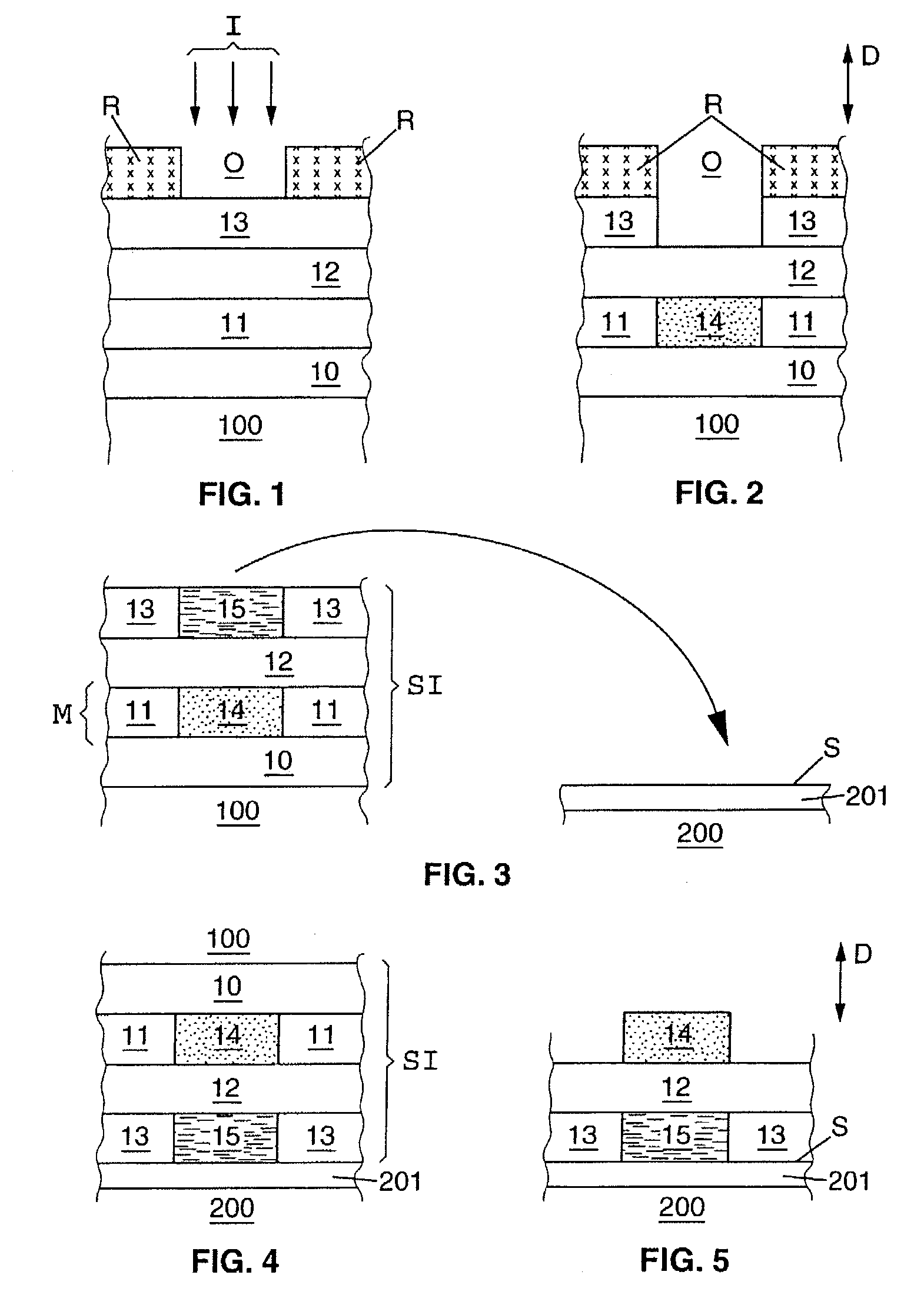
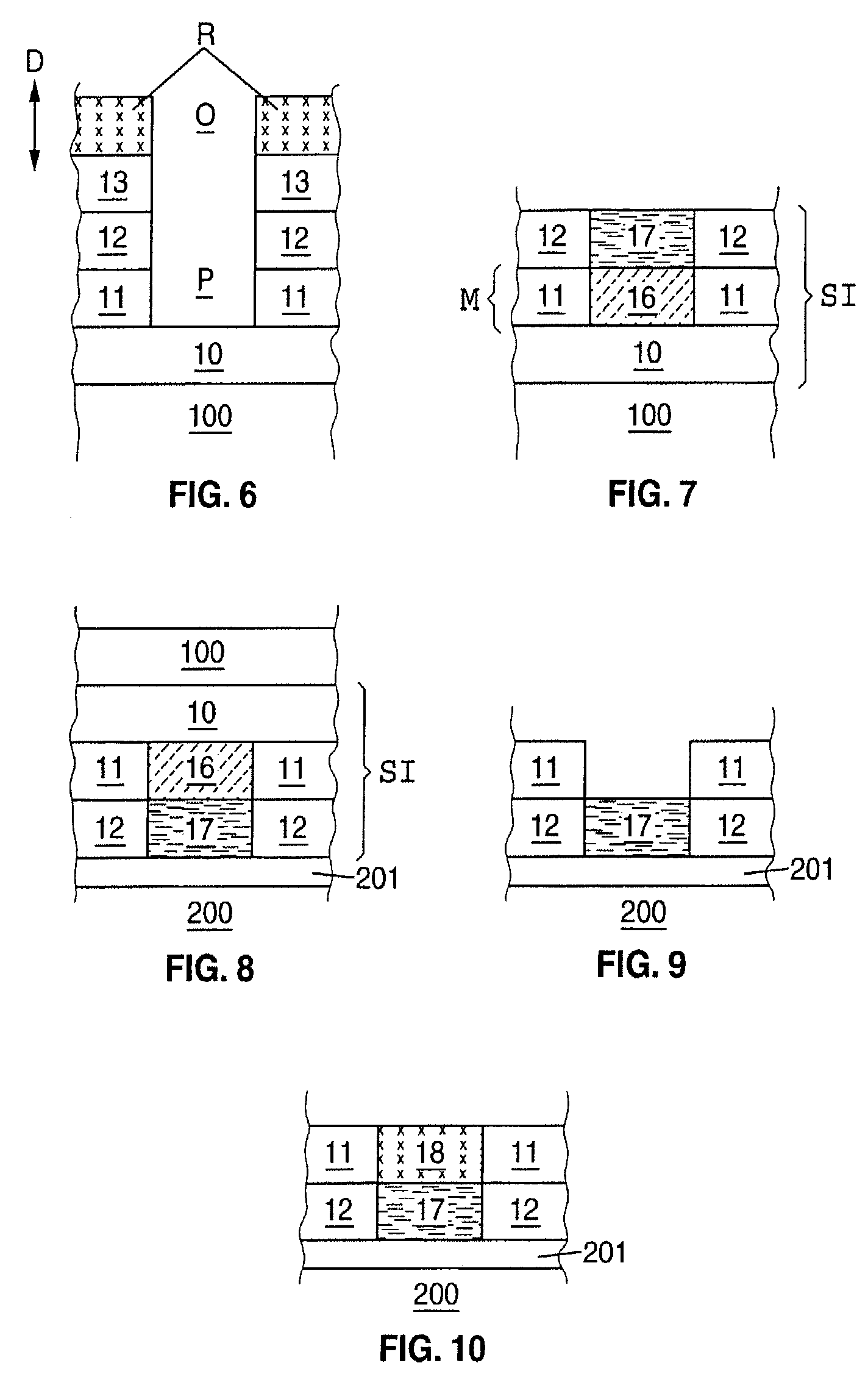
[0047]The production of a diode will now be described as the method of the present invention. The starting configuration is again the silicon substrate 100 covered with the layers 10–13 enumerated in the previous example, and with the resin mask R having the aperture O (FIG. 1). In this embodiment, the layer 11 is made of polycrystalline silicon. Optionally, a commercial SOI (silicon-on-insulator) substrate may be used, which includes a silicon base 100, the silica layer 10 and the upper silicon layer 11. Dry etching is carried out so as to hollow out, via the aperture O, a well P through the layer 13, the layer 12 and the layer 11 in succession along the direction D.

[0048]This etching is preferably carried out by successively exposing the structure of FIG. 1 to a plasma containing a gas such as sulfur hexafluoride (SF6) or hydrogen chloride (HCl) capable of etching the polycrystalline silicon, and then to a plasma containing a gas such as C4F8 capable of etching the silica. The sil...

first embodiment

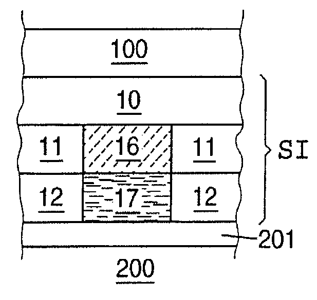
[0051]In the same way as in the first embodiment, the substrate 100 with the initial structure SI is then inverted and applied against the surface of a second substrate 200 covered with a silica layer 201. The surfaces of the layer 12 and of the volume 17 on the side opposite to the substrate 100 are thus brought into contact with that surface of the silica layer 201 which is on the side opposite to the substrate 200 (FIG. 8). In addition, the substrate 100 and the layer 10 are then removed, so as to expose those surfaces of the crystalline silicon layer 11 and of the volume 16 of silicon-germanium alloy that are on the opposite side to the substrate 200.

[0052]The selective treatment applied for this purpose at these exposed surfaces is preferably a selective wet etching treatment of the silicon-germanium alloy. Such selective etching uses, for example, an aqueous oxidizing solution composed of 40 milliliters of 70% nitric acid (HNO3), 20 milliliters of hydrogen peroxide (H2O2) and ...

third embodiment

[0054]the method of the present invention relates to the production of an MOS transistor having two gates placed on either side of a conduction channel. As is known, this type of transistor allows the current flowing in the channel to be controlled particularly precisely by the electrical potential applied to the gates. To do this, the two gates must be placed symmetrically with respect to the channel, by being correctly aligned with respect to each other, and with good reproducibility so as to reduce any dispersion in the electrical properties of the fabricated transistors.

[0055]The various process steps involved in the production of the transistor will not all be described in detail because their respective methods of implementation are well known. Only the chronological sequence according to the third embodiment of the present invention will be described.

[0056]FIG. 11 shows a crystalline silicon substrate 100 covered, in an order corresponding to the stack of the layers from the ...


PUM

PropertyMeasurementUnit
Structureaaaaaaaaaa
Volumeaaaaaaaaaa

Abstract

A method is provided for fabricating integrated electronic components. According to the method, an initial structure is produced on the surface of a first substrate. This initial structure incorporates a defined pattern formed from volumes of differentiated materials. At least part of the initial substrate that includes the defined pattern is transferred onto a second substrate, preferably by inverting the first substrate against the second substrate and then removing the first substrate. An additional structure is then produced on the second substrate. This additional structure includes volumes of material placed in correspondence with some of the volumes of differentiated material of the defined pattern. The electronic components thus produced may have a suitable configuration in accordance with technological or geometrical constraints. In a preferred method, a selective treatment is applied to the transferred part of the initial structure, so as to make a distinction between the volumes of differentiated material of the pattern.

Description

CROSS-REFERENCE TO RELATED APPLICATIONS[0001]This application is based upon and claims priority from prior French Patent Application No. 02-05073, filed Apr. 23, 2002, the entire disclosure of which is herein incorporated by reference.BACKGROUND OF THE INVENTION[0002]1. Field of the Invention[0003]The present invention relates to a method of fabricating integrated electronic circuits, and in particular to the production of complex structures intended to constitute parts of electronic components on the surface of a semiconductor substrate.[0004]2. Description of Related Art[0005]The production of electronic components on the surface of a semiconductor substrate results in general from a complex process which is subject to constraints of various types. Such constraints relate, for example, to the arrangement of the various components, or parts of components, with respect to one another, in order to allow these components to operate in the desired manner. Other constraints, of a geomet...

Claims


Application Information

Patent Timeline
IPC IPC(8): H01L21/46H01L21/30H01L21/02H01L21/3213H01L21/336H01L21/68H01L21/762H01L21/8242H01L23/544H01L27/12H01L29/78H01L29/786H01L51/00H01L51/40
CPCH01L21/32134H01L21/6835H01L21/76251H01L23/544H01L27/10852H01L27/1087H01L27/10873H01L27/1203H01L29/66484H01L29/66772H01L29/7831H01L29/78645H01L29/78648H01L2924/13091H01L28/91H01L51/0013H01L2221/68363H01L2223/54426H01L2223/54453H01L2224/83894H01L2924/19041H01L2924/01019H01L2924/01079H01L2924/00H10B12/0387H10B12/033H10B12/05H10K71/18
Inventor CORONEL, PHILIPPELEVERD, FRANCOISSKOTNICKI, THOMAS
Owner STMICROELECTRONICS SRL
Learn More