Optical interconnect architecture

a technology of optical interconnection and interconnection structure, applied in the field of opticalelectronic systems, can solve the problems of increasing the dielectric constant of insulating material, and increasing the cost of insulating material

a technology of optical interconnection and interconnection structure, applied in the field of opticalelectronic systems, can solve the problems of increasing the dielectric constant of insulating material, and increasing the cost of insulating material

US7215845B1Active Publication Date: 2007-05-08PHOTONIC

Image

  • Optical interconnect architecture
  • Optical interconnect architecture
  • Optical interconnect architecture

Examples


Embodiment Construction

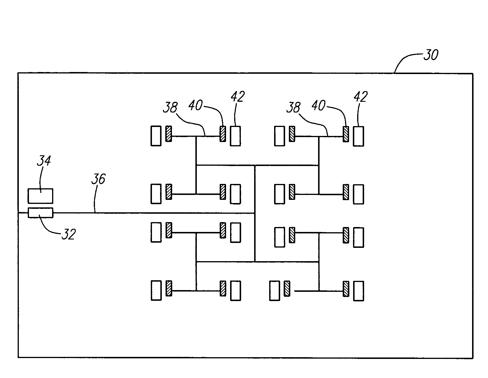
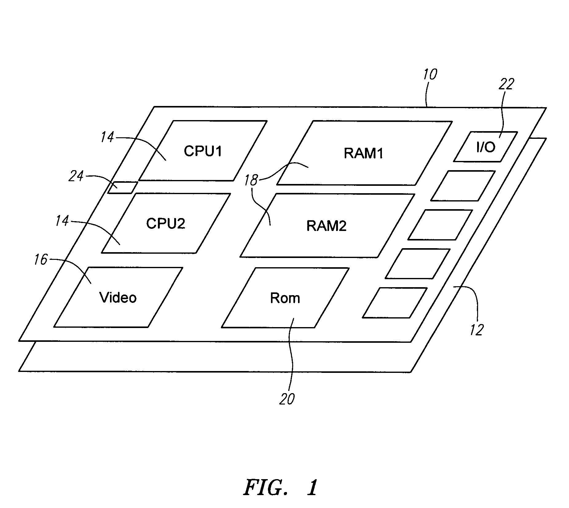
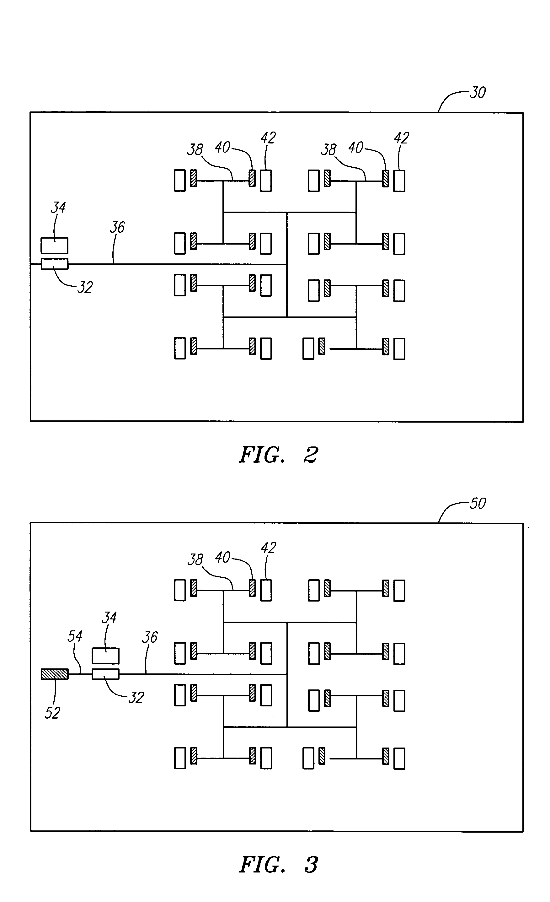
[0009]An aspect of the present invention provides an optical and electronic system, comprising an optical interconnect plane and an electronic plane. The optical interconnect plane includes a plurality of optical channels extending along a plane of the optical interconnect plane. The electronic plane includes first and second electronic circuits. First and second interlayer interconnects respectively couple signals to and from the first and second electronic circuits to the optical interconnect plane. A modulator on the optical interconnect plane receives signals from the first electronic circuit and modulates an optical signal in response to signals from the first electronic circuit and couples the optical signal to one of the optical channels. A receiver on the optical interconnect plane is coupled to the one of the optical channels to receive the optical signal and converts the optical signal into electronic signals coupled to the second electronic circuit on the electronic plane...


PUM


Abstract

An optical interconnect architecture provides three dimensional optical interconnects, with the optical interconnects provided along a plane such as a wafer or a substrate. One or more integrated circuits is provided on a second “electronic” plane that is spaced from the optical interconnect plane. Signals from the circuit on the electronic plane are coupled to the optical interconnect plane using various strategies, including metal or optical interlayer interconnects extending perpendicular to the optical plane. Once on the optical interconnect plane, the signals from the circuits on the electronic plane are propagated optically.

Description

BACKGROUND[0001]1. Field of the Invention[0002]The present invention relates to optical-electronic systems in which optical interconnects are used to distribute signals to or between one or more integrated circuit devices.[0003]2. Description of the Related Art[0004]Many modern integrated circuits are reaching limits on heat generation and adequate signal propagation, at least in part due to problems with interconnects. Advanced microprocessors are a good example. Signals are often carried within advanced microprocessors using copper wiring lines having lateral dimensions of substantially less than one micron. The resistance and density of these lines and the current carried by these lines are sufficient to make the interconnects a significant source of heating in the integrated circuit. Power dissipation and the increased margins required by excessive operating temperatures are problems for current integrated circuits and future circuit development is threatened by these problems.[...

Claims


Application Information

Patent Timeline
08 May 2007
Publication
US7215845B1
IPC
G02B6/293; G02B6/36
CPC
G02B6/12002; G02B6/43; G02B6/28
Inventors
CHAN, JAMES K.; DUTT, BIRENDRA