Equipment and method for manufacturing silicon carbide single crystal

a technology of silicon carbide and single crystal, which is applied in the direction of crystal growth process, polycrystalline material growth, chemically reactive gas, etc., can solve the problem of unsaturated gas, and achieve the effect of high efficiency, low raw material efficiency and high growth yield

Active Publication Date: 2007-05-15
DENSO CORP
View PDF9 Cites 5 Cited by
  • Summary
  • Abstract
  • Description
  • Claims
  • Application Information

AI Technical Summary

Benefits of technology

[0023]More preferably, the equipment further includes a tube for introducing the raw material gas toward the reactive chamber. The reactive chamber is separated from the tube. In this case, heat conduction is intercepted, so that the temperature difference between the tube of the heater and the reactive chamber can be set larger. If the temperature difference is large, degree of super saturation of the gas at the silicon carbide single crystal substrate as the seed crystal becomes larger. Thus, the growth yield of the crystal growth becomes higher.
[0024]Preferably, the equipment further includes a hydrogen separation film disposed on an outlet of the reactive chamber. The hydrogen separation film passes a hydrogen gas only. In this case, when the raw material gas introduced into the reactive chamber (i.e., the growth space) is discharged, the gas is filtered through the hydrogen separation film for passing only hydrogen gas. Therefore, only the hydrogen gas is selectively discharged. Thus, the raw material gas, which does not contribute to the crystal growth, is reused, so that the introduced raw material gas contributes to the crystal growth with high efficiency. Specifically, in the method of the prior art, the contribution rate of the raw material, which contributes to the crystal growth of the single crystal becomes small, so that the raw material efficiency becomes low. However, the above method and equipment resolve the problem of the low efficiency, so that the raw material efficiency is improved.

Problems solved by technology

Further, the crystal is not deposited on the upstream side and downstream side from the substrate since the upstream and downstream sides have high temperatures, at which unsaturated gas is provided.

Method used


Image

  • Equipment and method for manufacturing silicon carbide single crystal
  • Equipment and method for manufacturing silicon carbide single crystal
  • Equipment and method for manufacturing silicon carbide single crystal

Examples


first embodiment

[0056]A first embodiment of the present invention is described with reference to the drawings.

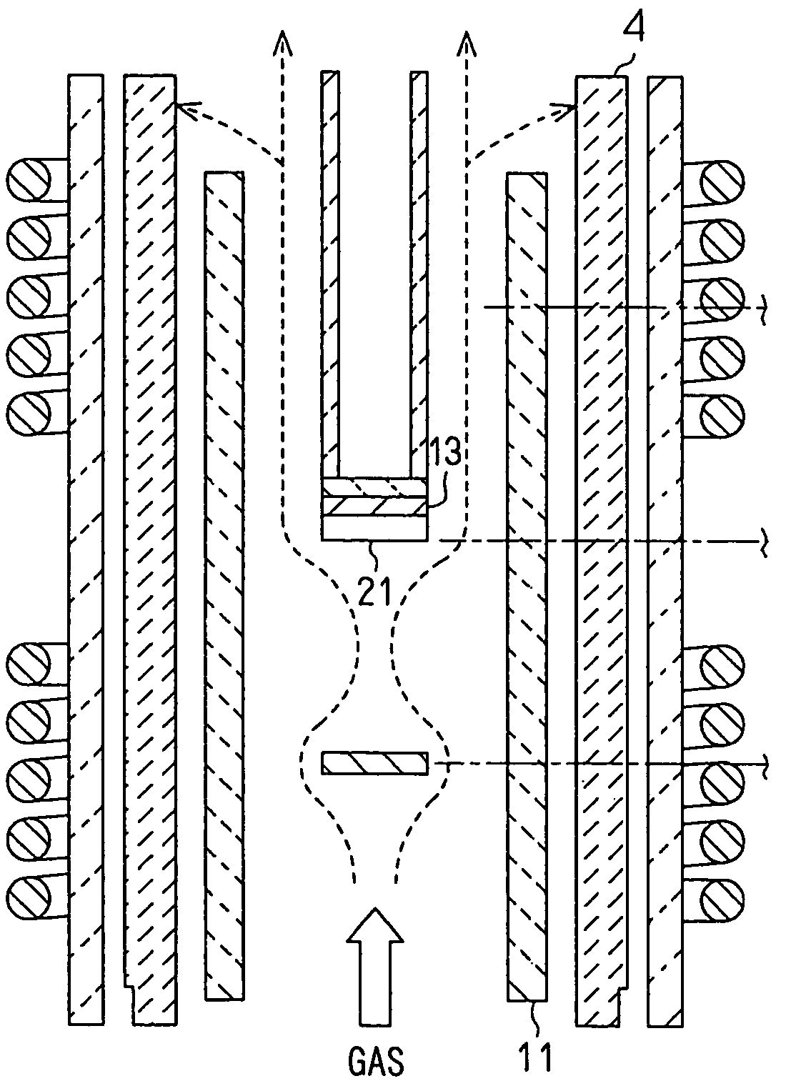
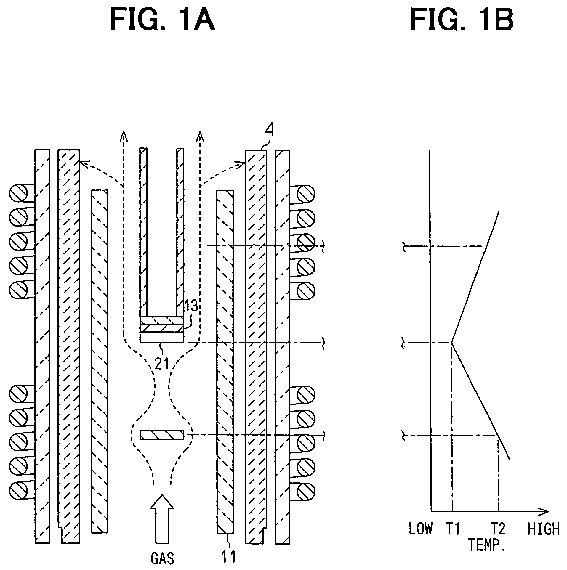
[0057]FIG. 1A is a schematic cross sectional view showing outline of equipment for manufacturing a silicon carbide single crystal, and FIG. 1B is a graph showing a relationship between a position and temperature in the equipment, according to a first embodiment of the present invention. FIGS. 1A and 1B explain a function of a method of the first embodiment. The method for manufacturing the silicon carbide single crystal shown in FIGS. 1A and 1B includes the steps of: setting a silicon carbide single crystal substrate 13 as a seed crystal in a reactive chamber 11; introducing a raw material gas including a silicon containing gas and a carbon containing gas into the reactive chamber 11; and growing a silicon carbide single crystal 21 from the silicon carbide single crystal substrate 13 as the seed crystal. The method is characterized in that the raw material gas is heated at an upstream side ...

second embodiment

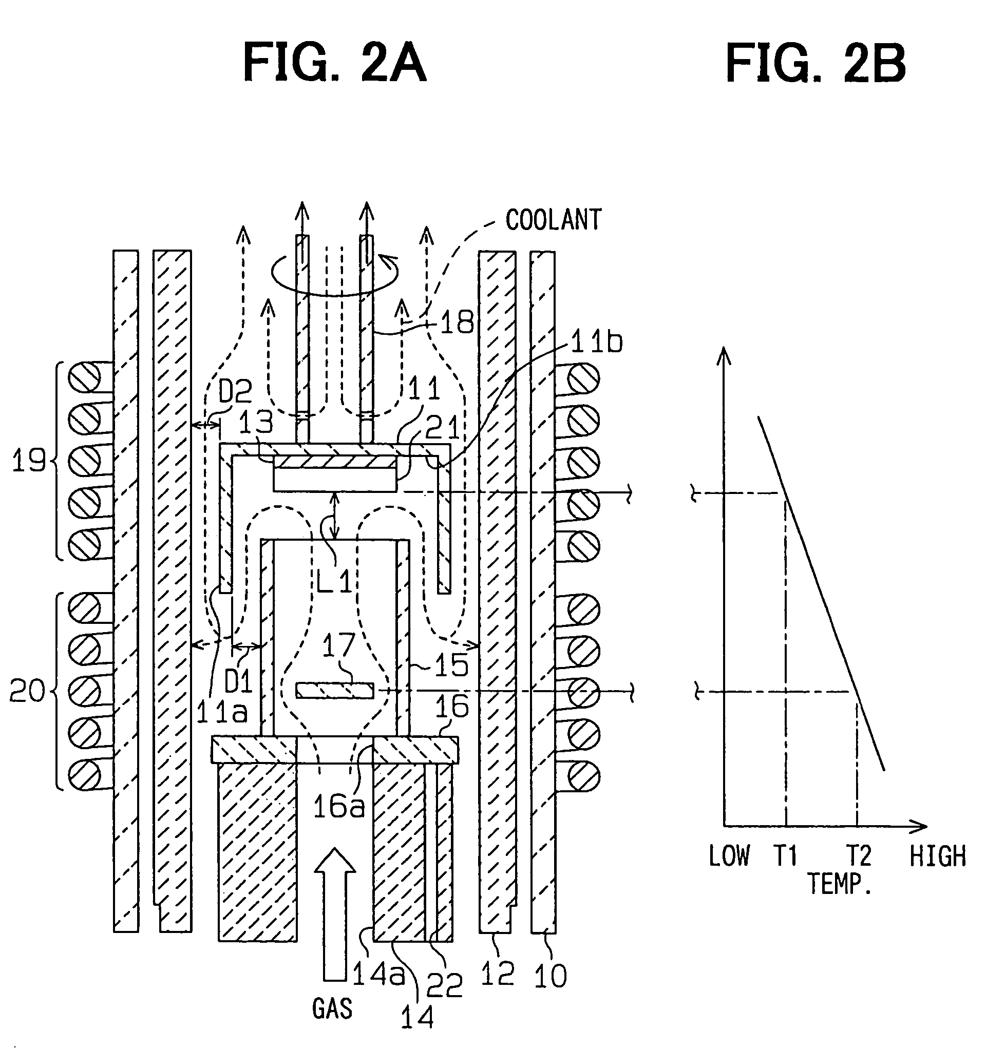
[0061]FIG. 2A is a schematic cross sectional view showing manufacturing equipment of a silicon carbide single crystal, according to a second embodiment of the present invention.

[0062]As shown in FIG. 2A, a vacuum chamber 10 is a cylinder, and disposed in a standing manner. The vacuum chamber 10 is made of, for example, quartz. A reactive chamber 11 is disposed in a standing manner inside the vacuum chamber 10. The reactive chamber 11 is a cylinder having a cover. The reactive chamber 11 is made of graphite. The reactive chamber 11 is composed of a cylinder 11a having a cylindrical shape and a cover 11b for covering an upper opening of the cylinder 11a (i.e., a lower end of the cylinder 11a is opened). A silicon carbide single crystal substrate 13 is mounted on the bottom of the cover 11b of the reactive chamber 11. The silicon carbide single crystal substrate 13 works as a seed crystal so that a silicon carbide single crystal 21 is deposited in the reactive chamber 11.

[0063]In the v...

third embodiment

[0091]Next, a third embodiment of the present invention is described. Specifically, difference between the second and third embodiments is described mainly.

[0092]FIG. 4 is a schematic cross sectional view showing manufacturing equipment of silicon carbide single crystal, according to the third embodiment.

[0093]In this embodiment, a plate 230 is used as a component of the heater (15, 16, 20) of the raw material gas. The plate 230 is disposed in a passage of the raw material gas in the tube 15, and has multiple through holes 231. The plate 230 is made of tantalum. The raw material gas passes through the through holes 231 of the plate 230 so that the gas is stirred. Thus, the stirred raw material gas is introduced into the reactive chamber 11 (i.e., the growth space) through the multiple through holes 231 of the plate 230. At that time, flow velocity of the raw material gas is different at each place. The raw material gas is heated at the upstream side from the silicon carbide single c...


PUM

PropertyMeasurementUnit
temperatureaaaaaaaaaa

Abstract

A method for manufacturing a silicon carbide single crystal includes the steps of: setting a substrate as a seed crystal in a reactive chamber; introducing a raw material gas into the reactive chamber; growing a silicon carbide single crystal from the substrate; heating the gas at an upstream side from the substrate in a gas flow path; keeping a temperature of the substrate at a predetermined temperature lower than the gas so that the single crystal is grown from the substrate; heating a part of the gas, which is a non-reacted raw material gas and does not contribute to crystal growth, after passing through the substrate; and absorbing a non-reacted raw material gas component in the non-reacted raw material gas with an absorber.

Description

CROSS REFERENCE TO RELATED APPLICATIONS[0001]This application is based on Japanese Patent Applications No. 2003-102016 filed on Apr. 4, 2003, and No. 2003-139387 filed on May 16, 2003, the disclosures of which are incorporated herein by reference.FIELD OF THE INVENTION[0002]The present invention relates to equipment and a method for manufacturing a silicon carbide single crystal.BACKGROUND OF THE INVENTION[0003]A silicon carbide single crystal has characteristics of high withstand voltage and high electron mobility. Therefore, the crystal is expected to use for a power device semiconductor substrate. The silicon carbide single crystal is formed by a single crystal growth method referred as a sublimation method (i.e., a modified Lely method).[0004]The modified Lely method is described as follows. A raw material of silicon carbide is disposed in a graphite crucible, which is almost closed and sealed. A seed crystal is mounted on an inner wall of the graphite crucible in such a manner ...

Claims


Application Information

Patent Timeline
Patent Type & Authority Patents(United States)
IPC IPC(8): C30B25/14C30B25/02
CPCC23C16/325C23C16/4412C23C16/45591C23C16/46C30B25/10C30B25/14C30B25/16C30B29/36C30B25/02Y10T117/10
Inventor SUGIYAMA, NAOHIROKITOU, YASUOMAKINO, EMIHARA, KAZUKUNIFUTATSUYAMA, KOUKIOKAMOTO, ATSUTO
Owner DENSO CORP
Why Eureka
Try Eureka