Three-dimensional temperature detector and manufacturing method for same

A technology of temperature detector and manufacturing method, which is applied in the field of semiconductors, can solve the problems of low yield rate, difficult process of suspension beam and suspension structure, etc., and achieve the effect of improving sensitivity, improving device performance and process stability

Active Publication Date: 2015-04-08
SHANGHAI IND U TECH RES INST
View PDF6 Cites 19 Cited by
  • Summary
  • Abstract
  • Description
  • Claims
  • Application Information

AI Technical Summary

Problems solved by technology

Among them, the process of cantilever beam and suspension structure is relatively difficult, and the yield rate is

Method used


Image

  • Three-dimensional temperature detector and manufacturing method for same
  • Three-dimensional temperature detector and manufacturing method for same
  • Three-dimensional temperature detector and manufacturing method for same

Examples


Embodiment 1

[0052] Embodiment 1 of the present application provides a method for manufacturing a three-dimensional temperature detector. Figure 6 It is a schematic flow chart of the manufacturing method of the three-dimensional temperature detector, and FIG. 7 is a schematic longitudinal sectional view of the device structure corresponding to each step of the manufacturing method of the three-dimensional temperature detector. Below, combine Figure 6 7, the manufacturing method of the three-dimensional temperature detector of this embodiment is described.

[0053] Step S601: depositing a first dielectric layer 10 on the substrate 9, such as Figure 7A shown.

[0054] In this embodiment, the substrate may be a wafer commonly used in the semiconductor manufacturing field, such as a silicon wafer, a silicon-on-insulator (Silicon-On-Insulator, SOI) wafer, a silicon-germanium wafer, a germanium wafer, or A gallium nitride (Gallium Nitride, GaN) wafer or the like, which is not limited in th...

Embodiment 2

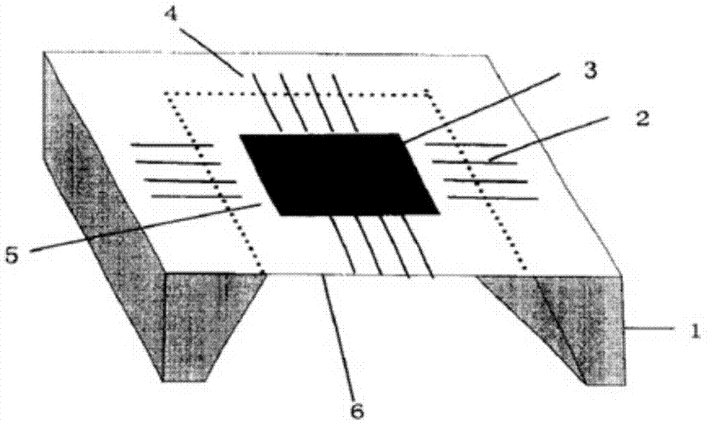
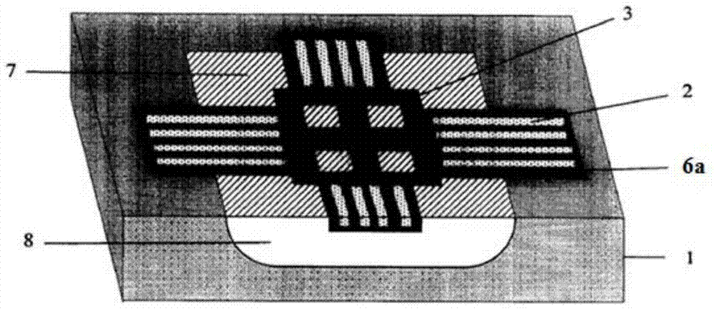
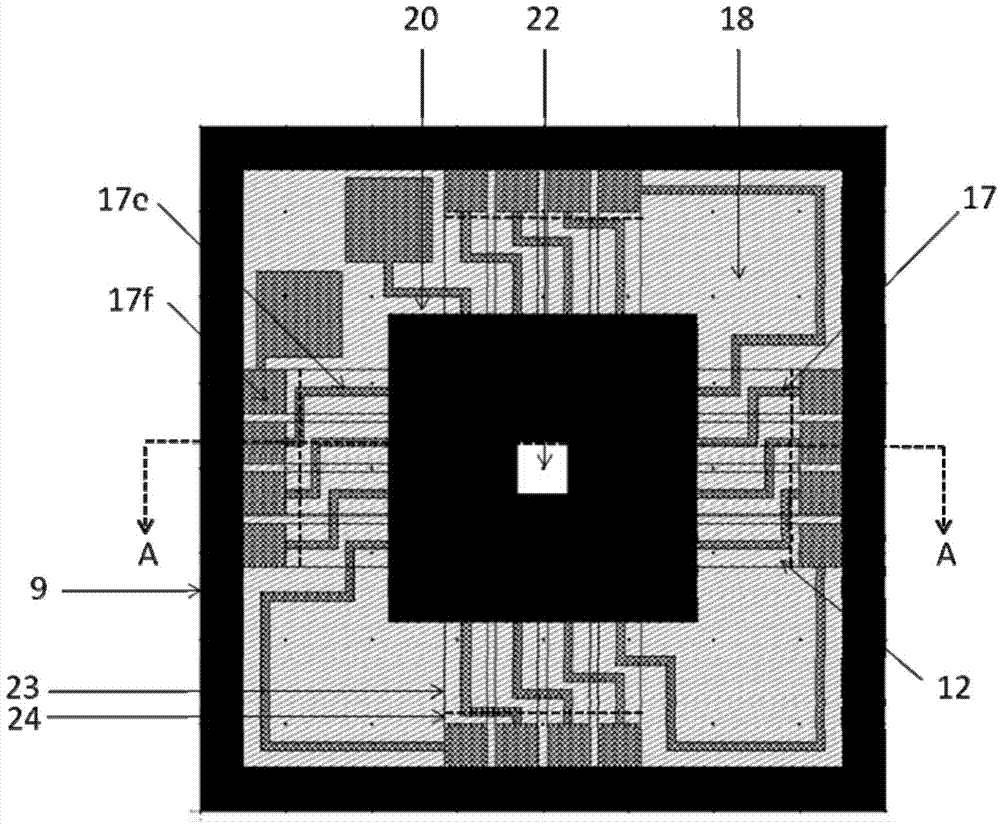
[0118] Embodiment 2 of the present application provides a three-dimensional temperature detector. image 3 is a schematic diagram of the top view structure of the three-dimensional temperature detector, Figure 4 is along image 3 The schematic diagram of the longitudinal section structure in the direction of A-A, Figure 5 It is a schematic diagram of the side view structure of the three-dimensional temperature detector. Such as Figure 3-5 As shown, the three-dimensional temperature detector includes:

[0119] Substrate (9);

[0120] A first dielectric layer 10 located on the surface of the substrate (9);

[0121] Located on the surface of the first dielectric layer 10, the first thermopile material structure 12, the second dielectric layer structure 14, the second thermopile material structure 17, and the third dielectric layer structure 18 are stacked sequentially from bottom to top , and, the first dielectric layer 10, the second dielectric layer structure 14, and t...


PUM

PropertyMeasurementUnit
Thicknessaaaaaaaaaa

Abstract

The invention provides a three-dimensional temperature detector and a manufacturing method for the same. The three-dimensional temperature detector comprises a substrate, a first dielectric layer positioned on the surface of the substrate and a cavity enclosed by the first dielectric layer, a first layer of thermoelectric pile material structure, a second dielectric layer structure, a second layer of thermoelectric pile material structure and a third dielectric layer structure, wherein a sixth groove and an infrared absorption layer structure filled in the sixth groove are arranged at the top of the cavity; the infrared absorption layer structure is provided with an eighth groove; the first layer of thermoelectric pile material structure is connected with the second layer of thermoelectric pile material structure through a fourth groove. According to the three-dimensional temperature detector and the manufacturing method for the same, the lengths of a thermoelectric pile thermocouple pair and a thermoelectric pile heat-insulating film can be increased to reduce the thermal conductivity, so that the temperature difference of a hot junction and a cold junction is increased, and the sensitivity of the temperature detector is improved; moreover, in a manufacturing process, process stability and device performance can be improved.

Description

technical field [0001] The present application relates to the field of semiconductor technology, in particular to a three-dimensional temperature detector and a manufacturing method thereof. Background technique [0002] Temperature detection has always been a hot topic in the sensor industry, among which infrared detection technology is more popular in design, manufacture and users due to its non-contact temperature measurement. As a kind of infrared detector, thermopile temperature sensor has been widely studied for its simple manufacturing process, low cost, convenient use, and no 1 / f noise. [0003] The main working principle of the thermopile temperature sensor is the Seebeck effect. This effect can be briefly described as: Two materials with different Seebeck coefficients (α1, α2) are connected at one end and open at the other end. If there is a temperature difference between the two ends ΔT=T1-T2, an open circuit potential ΔV will be generated at the open circuit end...

Claims


Application Information

Patent Timeline
IPC IPC(8): G01J5/12H01L35/34
CPCG01J5/12
Inventor 费跃王旭洪张颖
Owner SHANGHAI IND U TECH RES INST
Why Eureka
Try Eureka