Semiconductor device, module for optical devices, and manufacturing method of semiconductor device

a semiconductor and optical device technology, applied in the direction of cycle equipment, cycle stands, television systems, etc., can solve the problems of difficult to reduce the size of semiconductor devices and optical device modules, micro-lens parts, light receiving elements,

Active Publication Date: 2007-05-22
INVENSAS CORP
View PDF5 Cites 74 Cited by
  • Summary
  • Abstract
  • Description
  • Claims
  • Application Information

AI Technical Summary

Benefits of technology

[0053]Besides, since the semiconductor device of the present invention is smaller than a conventional semiconductor device with no through electrode, the prevent invention has advantageous effects, such as enabling a reduction in the size of a module for optical devices, comprising a small-sized semiconductor device.

Problems solved by technology

As a result, it is difficult to reduce the sizes of the semiconductor device and the module for optical devices.
In this case, there was a problem that the micro-lens part 114 or the light receiving element 113 was damaged.
In this case, there was a problem that the light incident through the glass lid 112 could not be accurately received by the light receiving element 113.
However, in order to seal the space between the glass lid 112 and semiconductor substrate 111 by securely bonding the adhesive part 127 and the glass lid 112 and semiconductor substrate 111, it is necessary to apply higher pressure to the glass lid 112 and the semiconductor substrate 111 compared to forming the adhesive part 127 by using an adhesive of low hardness, and therefore there is a possibility that the semiconductor substrate 111 will be damaged during the application of pressure.

Method used


Image

  • Semiconductor device, module for optical devices, and manufacturing method of semiconductor device
  • Semiconductor device, module for optical devices, and manufacturing method of semiconductor device
  • Semiconductor device, module for optical devices, and manufacturing method of semiconductor device

Examples


embodiment 1

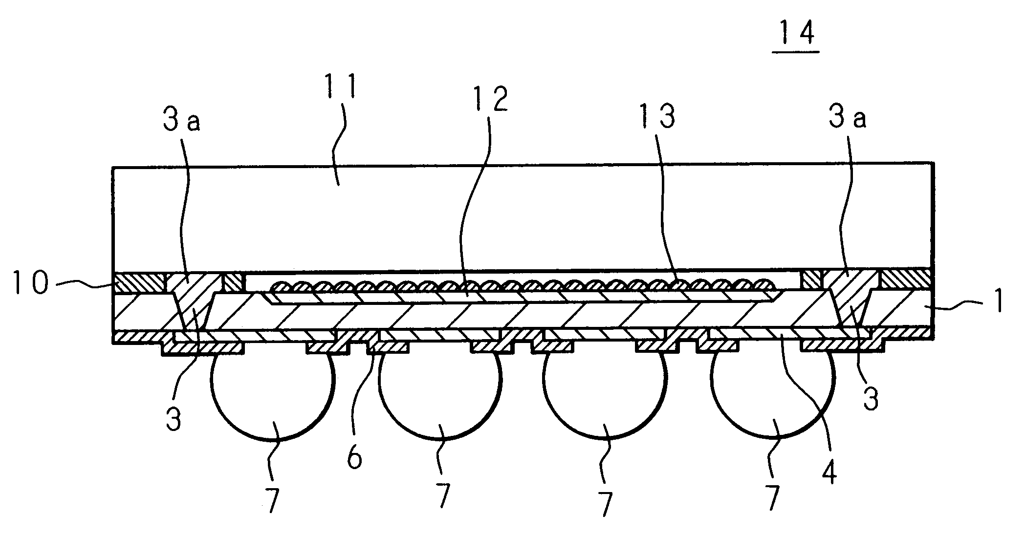
[0067]FIG. 4 is a plan view showing the structure of a semiconductor device 14 according to Embodiment 1 of the present invention. FIG. 5 is a cross sectional view showing the structure of the semiconductor device 14, and a cross section along the II—II line of FIG. 4. Further, FIG. 6 is an enlarged cross sectional view showing the structures of a through electrode 3 and a protruding part 3a of the semiconductor device 14, and an enlarged view of the vicinity of one through electrode 3 and protruding part 3a shown in FIG. 5. In FIG. 5, however, illustration of a through hole insulation film 2, a rear surface insulation film 5, an electrode pad 8, and a front surface protection film 9 shown in FIG. 6 is omitted.

[0068]As shown in FIGS. 4 and 5, the semiconductor device 14 comprises a semiconductor substrate 1 having a rectangular shape in the plan view. The semiconductor substrate 1 is a flat plate made of Si, for example, and an image pickup element 12 having a rectangular shape in t...

embodiment 2

[0117]FIG. 11 is a cross sectional view showing the structure of a semiconductor device 14 according to Embodiment 2 of the present invention. The difference between the semiconductor device 14 of this embodiment and that of Embodiment 1 is whether the semiconductor device 14 has the protruding parts 30, 30, . . . or not. Therefore, parts corresponding to Embodiment 1 are designated with the same reference codes, and explanations thereof are omitted.

[0118]The semiconductor substrate 1 has through electrodes 3, 3, . . . and protruding parts 3a, 3a, . . . which correspond one-to-one with each other. However, the number of the through electrodes 3, 3, . . . is smaller than the number of the through electrodes 3, 3, . . . in the semiconductor device 14 of Embodiment 1, or the layout of the through electrodes 3, 3, . . . is offset compared to the layout of the through electrodes 3, 3, . . . in the semiconductor device 14 of Embodiment 1, and consequently it is impossible to stably suppor...


PUM


Abstract

An image pickup element and a micro-lens part are formed on the front surface of a semiconductor substrate; through electrodes passing through the semiconductor substrate are formed; protruding parts protruding from the front surface toward a glass lid are formed in a thickness greater than the thickness of the micro-lens part on the through electrodes; and the protruding parts are interposed between the semiconductor substrate and the glass lid.

Description

CROSS-REFERENCE TO RELATED APPLICATIONS[0001]This non-provisional application claims priority under 35 U.S.C. §119(a) on Patent Application No. 2004-16296 filed in Japan on Jan. 23, 2004, the entire contents of which are hereby incorporated by reference.BACKGROUND OF THE INVENTION[0002]The present invention relates to a semiconductor device comprising a semiconductor substrate where a semiconductor element and a through electrode are formed, and a lid member attached to the semiconductor substrate, and also relates to a module for optical devices, and a manufacturing method of the semiconductor device.[0003]Conventionally, a package of CCD image sensor, CMOS image sensor or the like is used as a semiconductor device, and a sensor module such as a CCD image sensor, a CMOS image sensor or the like is used as a module for optical devices.[0004]FIG. 1 is a cross sectional view showing the structure of a conventional semiconductor device. A light receiving element 113 is formed in one su...

Claims


Application Information

Patent Timeline
Patent Type & Authority Patents(United States)
IPC IPC(8): H01L23/12H01L27/14H01L23/02H01L29/788H01L31/0203H01L31/0232H04N5/335H04N5/369
CPCH01L27/14618H01L27/14627H01L27/14636H01L27/14685H01L31/0203H01L31/0232H01L2924/3025H01L2924/01078H01L2924/01004H01L2224/73265H01L2224/48227H01L2224/32225H01L2224/48091H01L2924/00014H01L2924/00H01L31/02325H01L31/02327H01L2924/16195B62H1/12B62H7/00
Inventor ONO, ATSUSHIFUJIHARA, NORITO
Owner INVENSAS CORP
Why Eureka
Try Eureka