All-optical modulation device and method based on micro-nano GaAs optical waveguide

A technology of optical waveguide and modulation method, applied in optics, nonlinear optics, instruments, etc., can solve the problems of modulation extinction ratio limitation, not very strong, long recovery time of free carriers, etc., and achieve the effect of flexible control

Inactive Publication Date: 2012-09-05
HOHAI UNIV
View PDF5 Cites 8 Cited by
  • Summary
  • Abstract
  • Description
  • Claims
  • Application Information

AI Technical Summary

Problems solved by technology

At present, people study more on the use of the two-photon absorption effect in the micro-nano silicon-based optical waveguide with a highly nonlinear optical process to realize the all-optical modulation technology, but because the two-photon absorption process in the silicon medium is not very strong, Moreover, the free carriers generated by the two-photon absorption process have a long recovery time, so the optical modulation process in silicon-based optical waveguides is limited by the modulation extinction ratio and the operating rate.

Method used


Image

  • All-optical modulation device and method based on micro-nano GaAs optical waveguide
  • All-optical modulation device and method based on micro-nano GaAs optical waveguide
  • All-optical modulation device and method based on micro-nano GaAs optical waveguide

Examples


Embodiment

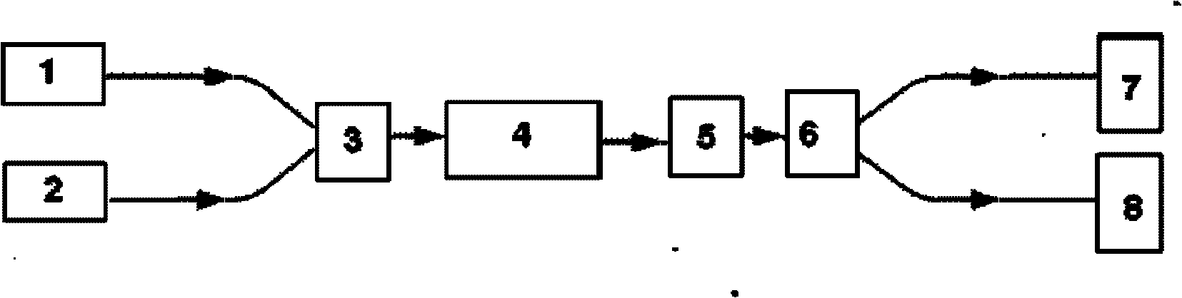
[0025] Embodiment: An all-optical modulation device based on a micro-nano GaAs optical waveguide, including a pumping laser light source 1, a continuous probe light laser source 2, a 2×1 fiber coupler 3, a micro-nano GaAs optical waveguide 4, and a filter 5 , 1 × 2 fiber coupler 6, spectrum analyzer 7 and pulse time domain analyzer 8, the pump light laser source 1, the continuous detection light laser source 2 are respectively connected to the input end of 2 × 1 fiber coupler 3 through optical fibers , the 2×1 fiber coupler 3, the micro-nano GaAs optical waveguide 4, the filter 5 and the 1×2 fiber coupler 6 are sequentially connected through optical fibers, and the output ends of the 1×2 fiber coupler 6 are respectively connected through optical fibers Connect with spectrum analyzer 7 and pulse time domain analyzer 8. The optical fiber is drawn into a 2×1 optical coupler 3 in a molten state, and a micro-nano GaAs optical waveguide 4 with excellent performance is prepared by we...


PUM

PropertyMeasurementUnit
lengthaaaaaaaaaa

Abstract

The invention discloses an all-optical modulation device based on a micro-nano GaAs optical waveguide. The all-optical modulation device comprises a laser light source, an optical fiber coupler, micro-nano GaAs optical waveguide and a filter, wherein the laser light source, the optical fiber coupler, the micro-nano GaAs optical waveguide and the filter are sequentially connected with one another through optical fibers. All-optical modulation signals realized by applying the all-optical modulation device has higher modulation depth and extinction ratio, the modulation rate reaches as high as dozens of Gb/s, and important performance parameters of modulated signals such as modulation depth and extinction ratio can be flexibly controlled by a pump light intensity adjusting method, a pump light-probe beam frequency detuning method and other methods. The all-optical modulation technology realized by the invention can be used in an integrated optoelectronic technology for effectively reducing the module scale of an optical modulator and improving the modulation rate and the modulation depth.

Description

technical field [0001] The invention relates to an all-optical modulation technology, in particular to an all-optical modulation device and method based on a micro-nano GaAs optical waveguide. Background technique [0002] All-optical modulation schemes based on various optical materials and devices have been widely developed and applied. With the rapid development of integrated optoelectronic technology, more and more people focus on the use of micro-nano optical dielectric waveguides with high nonlinear optical effects to realize all-optical modulation. modulation function. At present, people study more on the use of the two-photon absorption effect in the micro-nano silicon-based optical waveguide with a highly nonlinear optical process to realize the all-optical modulation technology, but because the two-photon absorption process in the silicon medium is not very strong, Moreover, the free carriers generated by the two-photon absorption process have a long recovery time...

Claims


Application Information

Patent Timeline
Patent Type & Authority Applications(China)
IPC IPC(8): G02F1/35
Inventor 吴建伟
Owner HOHAI UNIV
Why Eureka
Try Eureka