Electromagnetic interference shielding on semiconductor devices

a technology of electromagnetic interference and shielding, applied in the direction of electrical apparatus, electrical apparatus, electrical apparatus contruction details, etc., can solve the problems of increasing the overall size of the electronic package, increasing the cost of the device, and relatively expensive implementation of cvd

Inactive Publication Date: 2013-11-05
STMICROELECTRONICS PTE LTD
View PDF16 Cites 8 Cited by
  • Summary
  • Abstract
  • Description
  • Claims
  • Application Information

AI Technical Summary

Benefits of technology

[0012]The conductive paint EMI shield offers the advantages of providing effective EMI shielding that conforms to the shape of the module it protects, saving space and reducing the size of the module compared to known methods for EMI shielding of parts. The conductive paint EMI shield also costs less to implement compared with other methods, such as chemical vapor deposition coatings.

Problems solved by technology

However, CVD is relatively expensive to implement and therefore increases the cost of the device.
Although inexpensive to produce, the technique has the disadvantage of increasing the overall size of the electronic package.
While this method provides sound EMI shielding, the method increases the module assembly size and also increases production cost due to the complexity of the assembly process.

Method used


Image

  • Electromagnetic interference shielding on semiconductor devices
  • Electromagnetic interference shielding on semiconductor devices
  • Electromagnetic interference shielding on semiconductor devices

Examples


Embodiment Construction

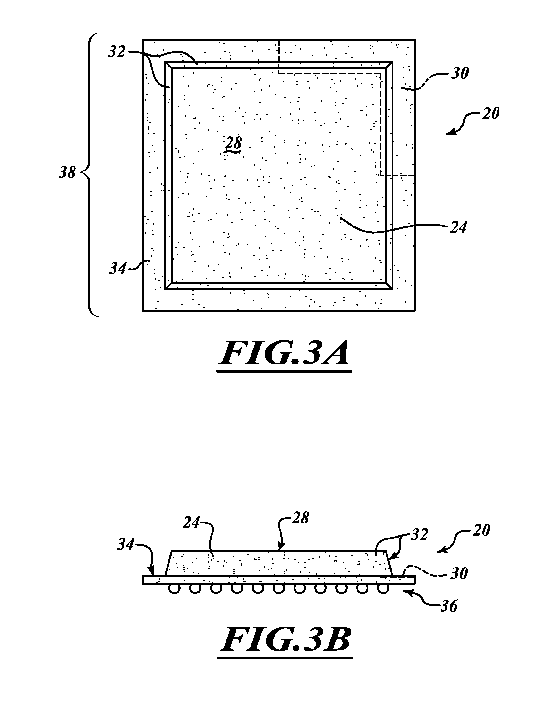
[0033]FIGS. 3A and 3B show top and side views of a ball grid array electronic package 20 having a conductive paint EMI shield 24 in accordance with principles of the present invention. In the embodiment of FIGS. 3A and 3B, the shielded electronic module 20 is a ball grid array electronic package. Any electronic module, including land grid array, dual-in-line package (DIP), quad flat package (QFP), flip chip, J-lead integrated circuit package, Power-SO package, multi-chip module, or any other of the many types of packages that can be used with this invention.

[0034]In the embodiment of FIGS. 3A and 3B, the ball grid array electronic package 20 includes the conductive paint EMI shield 24, a top surface 28, sidewalls 32, a perimeter ledge 34 and a ball grid array electrical interconnect 36. The top surface 28, sidewalls 32, and perimeter ledge 34 combine to form a total exposed surface 38 of the ball grid array electronic package 20. The ball grid array electrical interconnect 36 is on ...


PUM


Abstract

A conductive paint electromagnetic interference (EMI) shield for an electronic module or device. The conductive paint is composed of metal particles suspended in a fluidic carrier. In one embodiment, the conductive paint is sprayed onto exterior surfaces of an electronic module or device from a spray gun. The sprayed conductive paint is cured to remove the fluidic carrier, leaving a metal film coated to the outside of the module or device. In one embodiment used with electronic packages in array form, grooves are cut into an encapsulation material of a module so that the shield protection includes sidewalls of the package. In another embodiment used with camera modules, masking is used to selectively shield portions of the module. In a further embodiment, the shield is electrically connected to a ground conductor of a circuit of the electronic module.

Description

BACKGROUND[0001]1. Technical Field[0002]This description generally relates to the field of electronic devices and, in particular, to electromagnetic interference shielding of electronic devices.[0003]2. Description of the Related Art[0004]Electronic devices commonly require electromagnetic interference (EMI) shielding to prevent disruption of their performance due to electromagnetic fields in their operating environment. An EMI shield is typically one of a variety of metal containers that envelops an electronic device and is electrically connected to a ground reference of the device. The shield limits penetration of an EMI field to a circuit of the device by attenuating the EMI field before it reaches the device. The particular EMI shield selected for a device typically depends on the type of device requiring shielding.[0005]For packaged electronic devices, including ball grid array (BGA) electronic packages, one known shielding method uses sputtering. Sputtering, also known as chem...

Claims


Application Information

Patent Timeline
Patent Type & Authority Patents(United States)
IPC IPC(8): H05K1/18
CPCH01L21/561H01L21/565H01L23/3128H01L23/552H01L24/97H01L24/19H01L2224/04105H01L2224/20H01L2224/97H01L2924/01029H01L2924/01047H01L2924/01049H01L2924/01082H01L2924/19041H01L2924/3025H01L2224/81H01L2924/01023H01L2924/01033H01L2924/1815H01L2924/14H01L2924/00
Inventor WONG, WINGSHENQGANI, DAVIDDE LOS REYES, GLENN
Owner STMICROELECTRONICS PTE LTD
Why Eureka
Try Eureka