Package structure and the method to fabricate thereof

a packaging structure and manufacturing method technology, applied in the field of packaging structure, can solve the problems of poor modular capability, high cost and more development works of molding devices, and lack of modular capability, so as to improve electrical performance, reduce cost, and package structure better

Active Publication Date: 2013-08-22
CYNTEC
View PDF20 Cites 9 Cited by
  • Summary
  • Abstract
  • Description
  • Claims
  • Application Information

AI Technical Summary

Benefits of technology

[0011]Because the conductive pattern has been patterned in the substrate in an earlier process such as PCB manufacturing process which is much cheaper than film process (lithography process) or printing process, it can reduce cost significantly.
[0012]The substrate is modifiable or replaceable. In one embodiment, if there is a failure of the conductive pattern in the substrate, the substrate can be removed and a portion of the conductive pattern in the substrate can be repaired or modified. In one embodiment, a portion of the conductive pattern in the substrate can be repaired or modified without removing the substrate from the package structure. In one embodiment, the substrate can be replaced with the another substrate having another conductive pattern therein in order to have better package structure and better electrical performance.

Problems solved by technology

However, such kind of conventional process has many disadvantages including: a. higher cost and more development works of molding devices; b. poor capability in area design which is only in the form of plane so that product size doesn't shrink; c. lacking of modular capability as it is only good for packaging a single device; and d. poor performance in heat dissipation.
Conventionally, if the conductive pattern in the package structure needs to be modified or changed, it can't be repaired in the conductive pattern locally.
Moreover, the package structure can't be easily disassembled and combined.

Method used


Image

  • Package structure and the method to fabricate thereof
  • Package structure and the method to fabricate thereof
  • Package structure and the method to fabricate thereof

Examples


Embodiment Construction

[0027]The detailed explanation of the present invention is described as following. The described preferred embodiments are presented for purposes of illustrations and description and they are not intended to limit the scope of the present invention.

[0028]To make the following description clear in the present invention, some words inclined to be confusing are defined in the beginning A device carrier means an object on which at least one device is disposed. Depending on size, shape or location of the device, the device carrier can have any suitable appearance

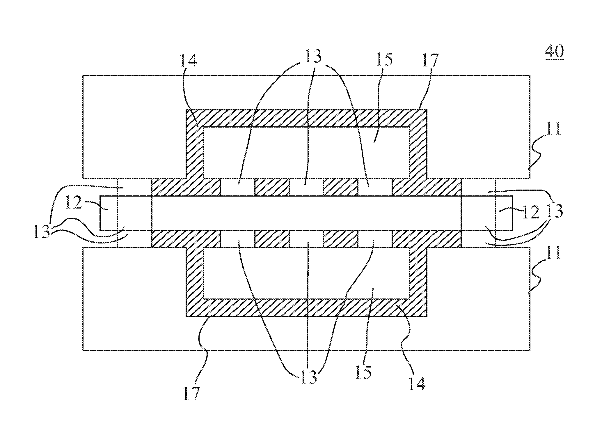
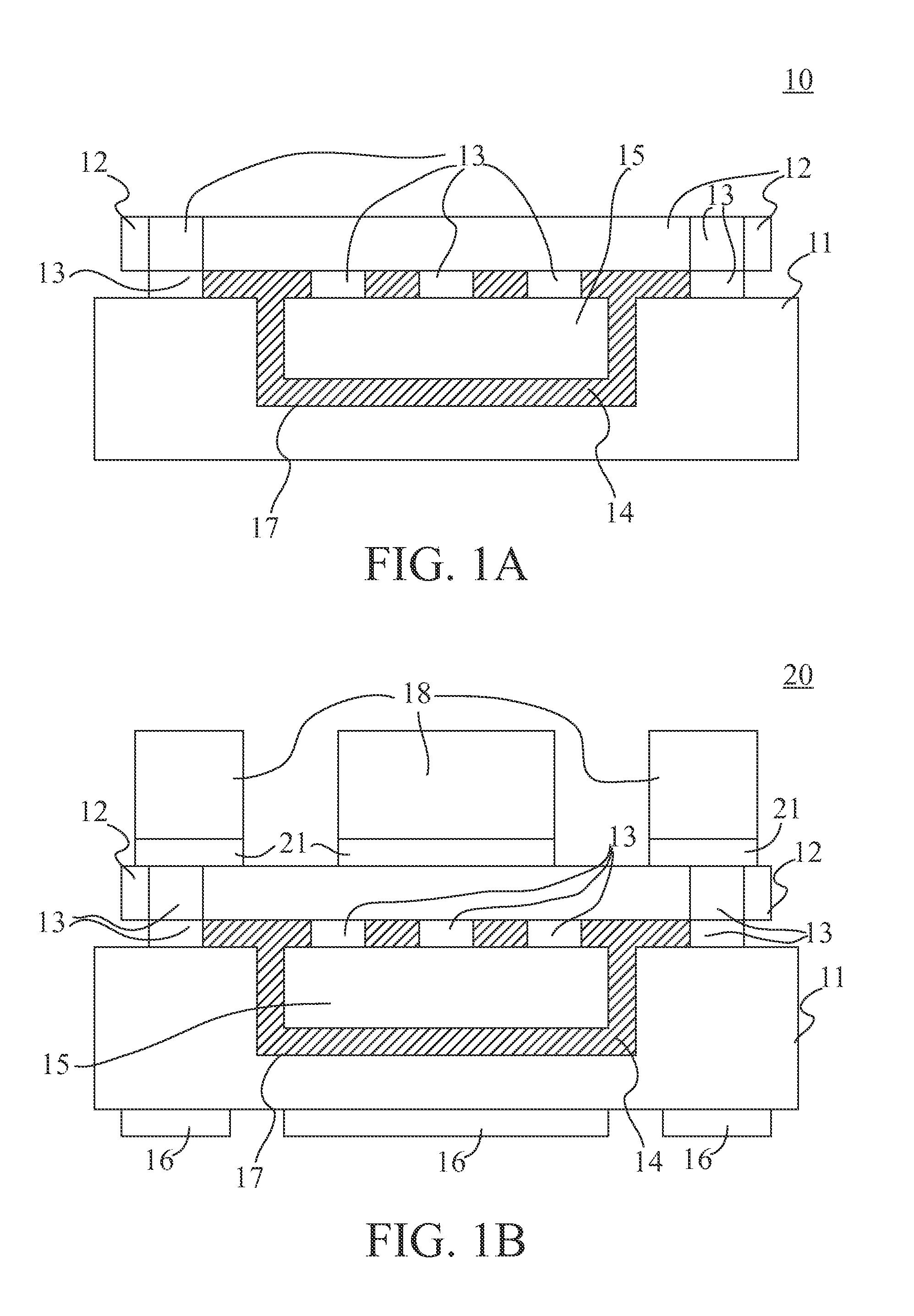
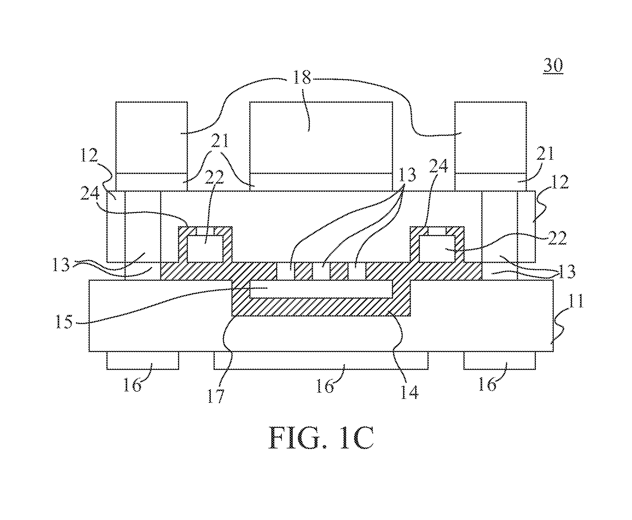
[0029]The invention discloses a package structure made of the combination of a device carrier and a modifiable substrate. FIG. 1A illustrates a schematic cross-sectional view of the package structure 10. The structure 10 includes a device carrier 11, a substrate 12, a conductive pattern 13, an insulating layer 14, and a first conductive element 15.

[0030]A device carrier 11 has a conductive pattern (not shown) therein and a plural...


PUM

PropertyMeasurementUnit
conductiveaaaaaaaaaa
metallicaaaaaaaaaa
insulatingaaaaaaaaaa

Abstract

The invention discloses a package structure made of the combination of a device carrier and a modifiable substrate. In one embodiment, a recess is formed in the device carrier and a conductive element is disposed on the substrate, wherein the substrate is disposed on the device carrier and the conductive element is located in the recess of the device carrier. The conductive pattern in the substrate is electrically connected to the device carrier and I/O terminals of the first conductive element. The invention also discloses a method for manufacturing a package structure made of the combination of a device carrier and a modifiable substrate. In one embodiment, a portion of the conductive pattern in the substrate can be modified.

Description

BACKGROUND OF THE INVENTION[0001]I. Field of the Invention[0002]The present invention relates to a package structure and, in particular, to a package structure made of the combination of a device carrier and a modifiable substrate.[0003]II. Description of the Prior Art[0004]Lead frame is a material for IC package and can be in variety of forms such as QFP, TSOP, SOT or SOJ. The molded semiconductor devices are constructed by assembling and interconnecting a semiconductor device to a lead frame. The structure is often molded with plastic material. A lead frame is made by a metal ribbon with a paddle (also known as a die paddle, die-attach tab, or island) for attaching a semiconductor device thereto and a plurality of leads arranged in a manner such that the leads do not overlap the paddle on which the semiconductor device is to be mounted.[0005]Conventionally, lead frame is used for die bond of an IC chip. The process flow includes many stages which are wire bond, molding of IC chip,...

Claims


Application Information

Patent Timeline
Patent Type & Authority Applications(United States)
IPC IPC(8): H05K1/11H05K3/00
CPCH01L24/16H01L2924/13055H01L2924/13091H01L23/49833H01L2224/16225H01L2924/15321H01L21/563H05K1/021H05K1/186Y10T29/49124H01L23/13H01L23/49827H01L2924/00H01L23/49506H01L23/49534H01L23/49537H01L23/49548H01L23/49575
Inventor LU, BAU-RULI, JENG-JENSHIH, KUN-HONGCHIANG, KAIPENG
Owner CYNTEC
Why Eureka
Try Eureka