Semiconductor device, method for manufacturing the same, liquid crystal television and EL television

a semiconductor and semiconductor technology, applied in the field of semiconductor devices, can solve the problems of deterioration of throughput, waste of gate electrode and resist materials, and difficulty in the use of exposure devices for photolithography process, and achieve the effect of high usability of materials

Inactive Publication Date: 2007-05-29
SEMICON ENERGY LAB CO LTD
View PDF42 Cites 41 Cited by
  • Summary
  • Abstract
  • Description
  • Claims
  • Application Information

AI Technical Summary

Benefits of technology

[0009]In view of the foregoing, it is an object of the present invention to provide a method for manufacturing a semiconductor device by a small number of processes and by a means by which high usability of materials is realized.
[0030]According to the present invention, filling the gaps of a plurality of the conductive layers by the insulating layer can reduce irregularities of the gate insulating film formed over the insulating layer, and so step coverage can be improved. Therefore, step cut over conductive edges can be prevented, and manufacturing yields of the semiconductor device having the conducive layer and the gate insulating film can be improved.
[0031]Since the semiconductor device according to the present invention can increase the uniformity of the thickness of the gate insulating layer, the resistance to pressure of the gate insulating film can be improved and the reliability of the semiconductor device can also be improved.
[0033]By forming the insulating film that fills the gaps of a plurality of the conductive layers by droplet discharging, droplets can be dropped to a predetermined place by varying the relative positions of a substrate and a nozzle that is a discharge opening of the droplets containing a material of these films. The relative relationship among a nozzle diameter, a discharge rate of a droplet, and movement speed of the nozzle and the substrate discharged with the droplets can adjust the thickness or the width of a pattern to be formed. Therefore, an insulating film can be formed by discharging with high accuracy at a desired place even when a large substrate with a side of 1 to 2 m or more is used. Further, the number of manufacturing processes can be reduced, the throughput can be increased, and the cost can be reduced since the insulating layer can be formed at a predetermined place without using a photolithography process.
[0034]Moreover, a liquid crystal television and an EL television having the semiconductor device manufactured by the foregoing processes can be manufactured at low costs with high throughput and high manufacturing yields.

Problems solved by technology

Therefore, there have been problems that most materials for the gate electrode and the resist are wasted, and throughput becomes deteriorated since a large number of processes for forming the resist mask pattern and the gate electrode is required in a manufacturing process of a semiconductor device.
It is difficult for an exposure device used for the photolithography process to perform exposure processing of a large substrate at once.
Therefore, a manufacturing method of a semiconductor device using a large substrate has problems that exposure processing is required to be performed at a plurality of times and manufacturing yields are deteriorated due to a mismatch between adjacent patterns.

Method used


Image

  • Semiconductor device, method for manufacturing the same, liquid crystal television and EL television
  • Semiconductor device, method for manufacturing the same, liquid crystal television and EL television
  • Semiconductor device, method for manufacturing the same, liquid crystal television and EL television

Examples


embodiment 1

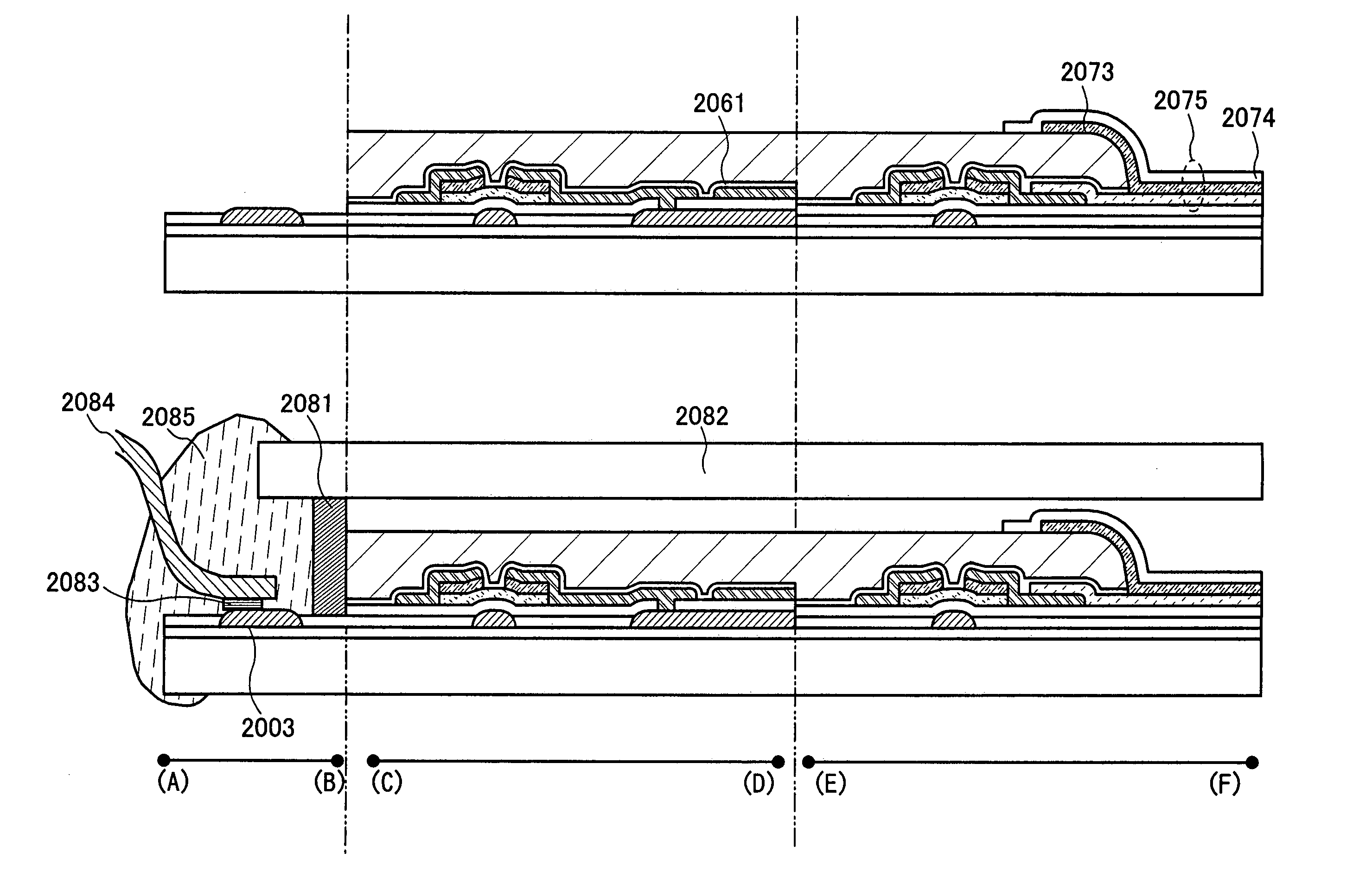
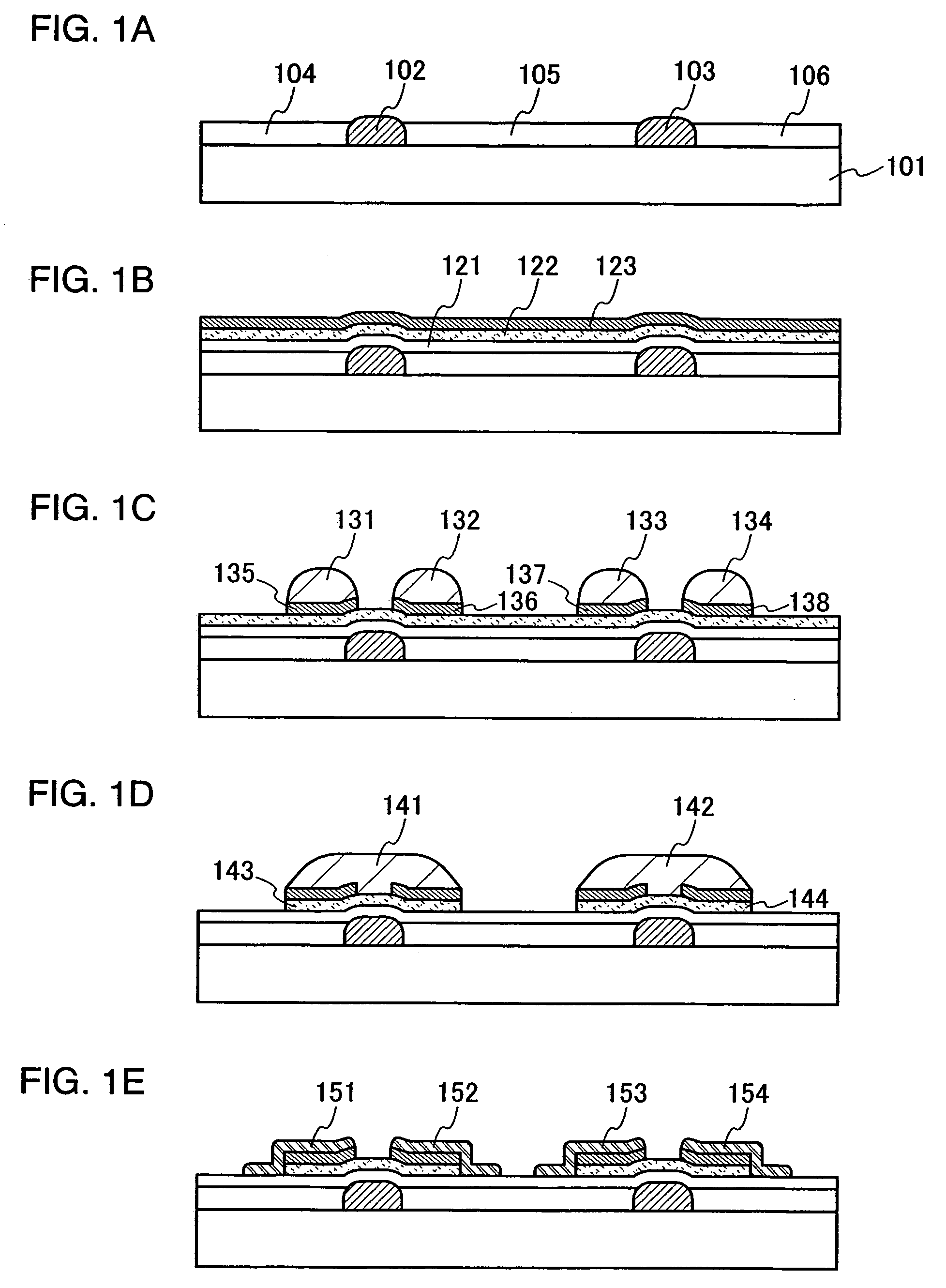
[0075]In this embodiment, a semiconductor device, which includes an insulating layer for filling between a plurality of conductive layers, and which has lower height than that of the conductive layers, and a manufacturing process of the semiconductor device are explained with reference to FIGS. 1A to 1E, 4A, 4B, 7A, and 39A. In this embodiment, a channel etch TFT is used in a bottom gate TFT as a semiconductor device.

[0076]As illustrated in FIG. 1A, a plurality of first conductive layers 102, 103 is formed over a substrate 101, and first insulating layers 104 to 106 are formed to fill between the plurality of the first conductive layers 102, 103.

[0077]As the substrate 101, a substrate made from an insulating substance such as glass, quartz, or alumina; a plastic substrate having heat resistance that can resist processing temperature in the following process; a silicon wafer, a metal plate, or the like can be used. In this instance, an insulating film for preventing impurities from d...

embodiment 2

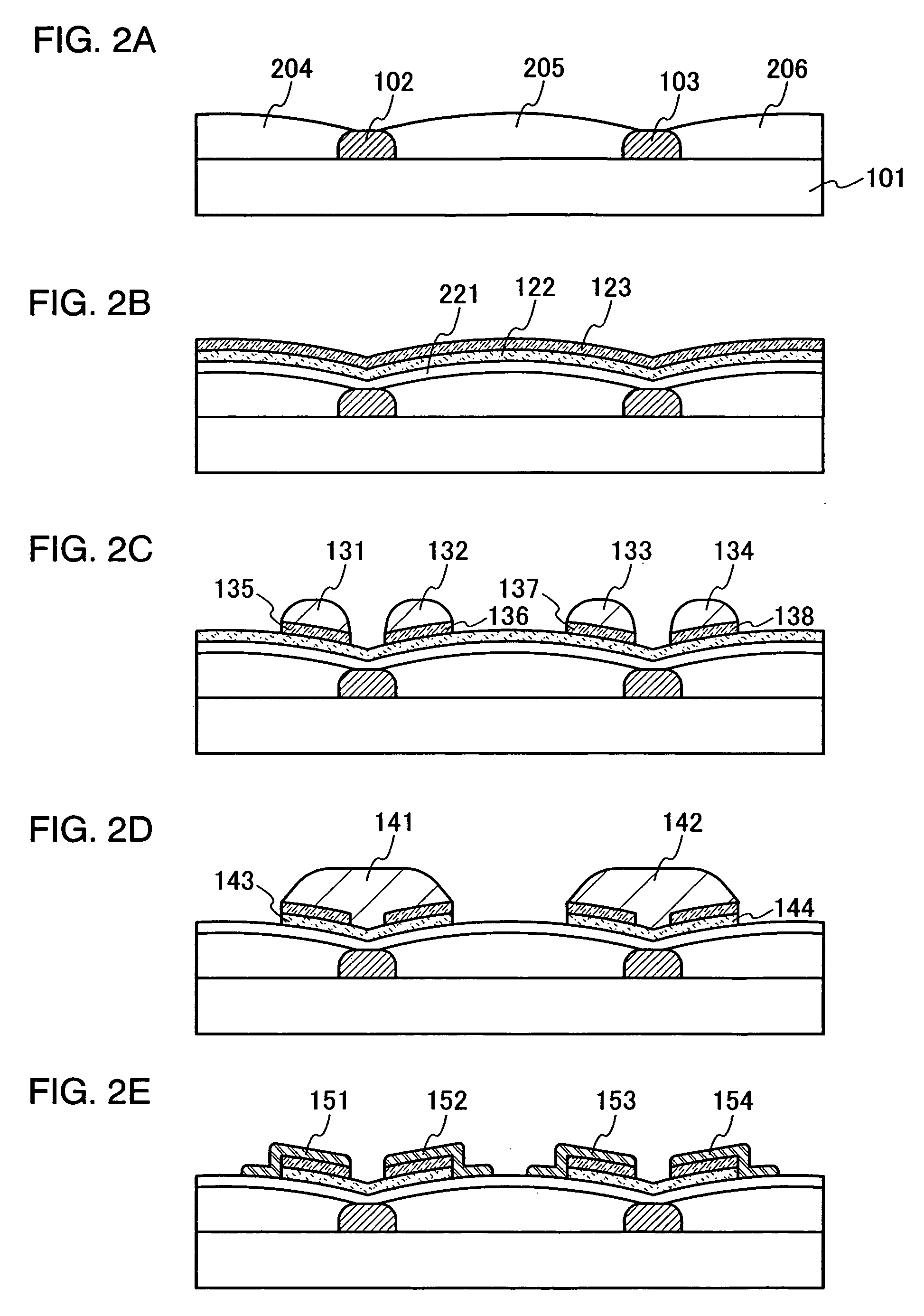
[0122]In this embodiment, a process for manufacturing a semiconductor device in Embodiment 1 in which a first insulating layer has a larger thickness than that of a first conductive layer is explained with reference to FIGS. 2A, 2B, 7B, and 39B. In this embodiment, a channel etch TFT in a bottom gate TFT is explained as the semiconductor device.

[0123]As illustrated in FIG. 2A, first conductive layers 102, 103 are formed over a substrate 101 as is the case with Embodiment 1. Then, first insulating layers 204 to 206 are formed. The first insulating layers 204 to 206 have larger thicknesses than those of the first conductive layers 102, 103 and cover a part of the side and top of the first conductive layers 102, 103.

[0124]The first insulating layers 204 to 206 can be formed by the same material and the same method as those of the first insulating layers 104 to 106 in Embodiment 1.

[0125]As illustrated in FIG. 2B, a second insulating layer 221, a first semiconductor film 122, and a secon...

embodiment 3

[0132]The shapes of first conductive layers 102, 103 that can be applied to the present invention in Embodiment 1 or 2 are explained with reference to FIGS. 3A to 3E. This embodiment gives an explanation with Embodiment 2. Further, Embodiment 1 can also be appropriately used.

[0133]As illustrated in FIG. 3A, a conductive film having a tapered portion with a contact angle θ1 of 70 to 90° against a substrate 101 at an edge portion, that is, a conductive layer 301 is formed to have a cross-section in a trapezoidal shape, and first insulating layers 204, 205 are formed. Conventionally, there have been problems that a step coverage property of a film is deteriorated and stepped cut is produced with the increase of a contact angle in the case of the film is formed over a film pattern having a contact angle θ1 of 70° or more. However, the stepped cut of a film formed afterwards can be prevented and the uniformity of a film thickness can be improved by forming the first insulating layers 204...


PUM


Abstract

A method for manufacturing a semiconductor device by a small number of processes and by a means with high usability of materials to have high-definition and a gate insulating with a high step coverage property is disclosed. According to the present invention, a method for manufacturing a semiconductor device comprises the steps of forming a plurality of first conductive layers over a substrate; forming a first insulating layer to fill the gaps of the plurality of the first conductive layers; forming a second insulating layer over the first insulating layer and the plurality of the first conductive layers; and forming a semiconductor region and a second conductive layer over the second insulating layer.

Description

BACKGROUND OF THE INVENTION[0001]1. Field of the Invention[0002]The present invention relates to a semiconductor device formed by droplet discharging as typified by an ink jetting method, and a method for manufacturing the semiconductor device.[0003]2. Related Art[0004]Conventionally, a so-called active matrix driving display panel or a semiconductor integrated circuit, each of which is composed of a semiconductor element as typified by a thin film transistor (hereinafter, TFT) over a glass substrate, is manufactured by patterning a various kinds of thin films by a light exposure process using a photomask (hereinafter, photolithography process).[0005]By the photolithography process, resist is coated allover the surface of a substrate to be pre-baked, and an ultraviolet ray or the like is emitted thereto via a photomask, then, a resist pattern is formed by developing. Thereafter, a thin film (that is formed by a semiconductor material, an insulating material, or a conducting material...

Claims


Application Information

Patent Timeline
Patent Type & Authority Patents(United States)
IPC IPC(8): H01L21/84H01L21/00H01L21/425H01L21/8238H01L21/8242H01L21/77H01L27/12H01L27/32H01L29/423H01L29/786H01L31/0392
CPCH01L27/1292H01L27/12H01L29/42384H01L29/78603G02F2001/13685G03F1/82H01L2924/07811H01L2924/10253H01L2924/01055H01L2924/01019H01L2924/3025H01L2924/19041H01L2924/04941H01L27/3244H01L2224/16225H01L2224/48091H01L2224/48465H01L2224/73204H01L2924/01004H01L2924/01012H01L2924/0102H01L2924/01025H01L2924/01029H01L2924/01046H01L2924/01077H01L2924/01078H01L2924/01079H01L2924/00014H01L2924/00H01L2924/12044H01L2224/05024H01L2224/05008H01L2224/05001H01L2224/05572H01L2224/05166H01L2224/05181H01L2224/05644H01L24/05G02F1/13685H10K59/12
Inventor MAEKAWA, SHINJI
Owner SEMICON ENERGY LAB CO LTD
Why Eureka
Try Eureka