
Resettable fuse device and method of fabricating the same

a fuse device and resettable technology, applied in semiconductor devices, semiconductor/solid-state device details, electrical apparatus, etc., can solve problems such as permanent change, inoperable rendering of bad locations, and the need to scrap entire devices

Inactive Publication Date: 2007-06-05
GOOGLE LLC
View PDF2 Cites 2 Cited by
  • Summary
  • Abstract
  • Description
  • Claims
  • Application Information

AI Technical Summary

Benefits of technology

This patent describes a resettable fuse device and a method for fabricating it. The device includes a gate region, a source node, an extension region, and a drain node. The device can be used in semiconductor devices and can be programmed by applying a predetermined bias voltage to the drain node. The method includes steps of etching a hard mask, implanting impurities, and removing the hard mask and sidewall spacers. The device can be used in various semiconductor devices and can be programmed by applying a predetermined bias voltage to the drain node.

Problems solved by technology

If in the process of testing during the manufacturing cycle, a defective memory location is detected, the appropriate hard fuse can be severed, rendering the bad location inoperable.
While simple to fabricate, a disadvantage of the hard fuse is that the change is permanent.
Moreover, once the RAM cell array is sealed after testing, any further failures of memory locations cannot be cannot corrected by severing fuse links, and the entire device may have to be scrapped.
Another disadvantage of hard fuses is they are severed by laser cutting and therefore must be placed away from other sensitive parts of the chip.
This tends to increase the distance that signals on the data lines must travel, an undesirable feature in high speed, high density, microelectronic circuits.

Method used


Image

  • Resettable fuse device and method of fabricating the same
  • Resettable fuse device and method of fabricating the same
  • Resettable fuse device and method of fabricating the same

Examples


Embodiment Construction

[0029]The invention will now be described in more detail by way of example with reference to the embodiments shown in the accompanying figures. It should be kept in mind that the following described embodiments are only presented by way of example and should not be construed as limiting the inventive concept to any particular physical configuration.

[0030]Further, if used and unless otherwise stated, the terms “upper,”“lower,”“front,”“back,”“over,”“under,” and similar such terms are not to be construed as limiting the invention to a particular orientation. Instead, these terms are used only on a relative basis.

[0031]The present invention is directed toward a simple resettable fuse device that can be used in digital and analog integrated circuits for the adding or removing circuit elements on a dynamic basis.

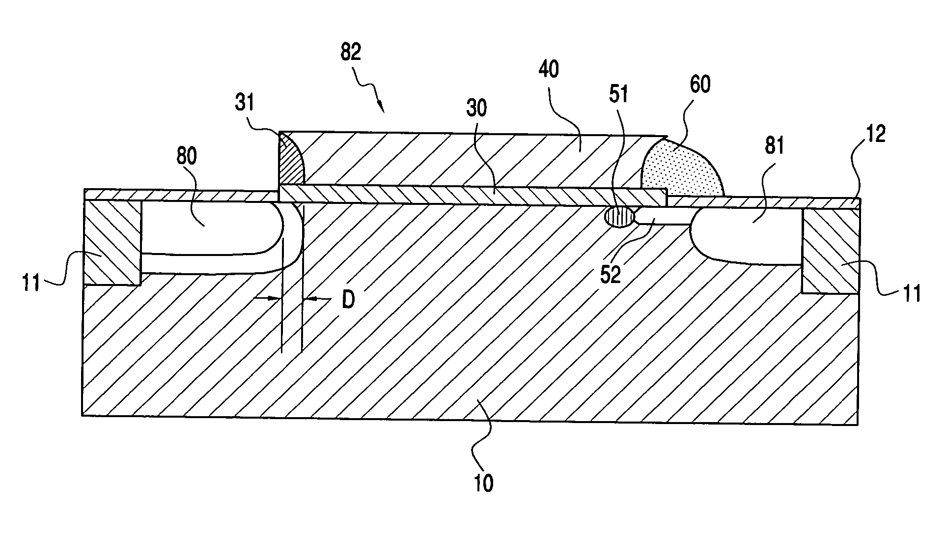
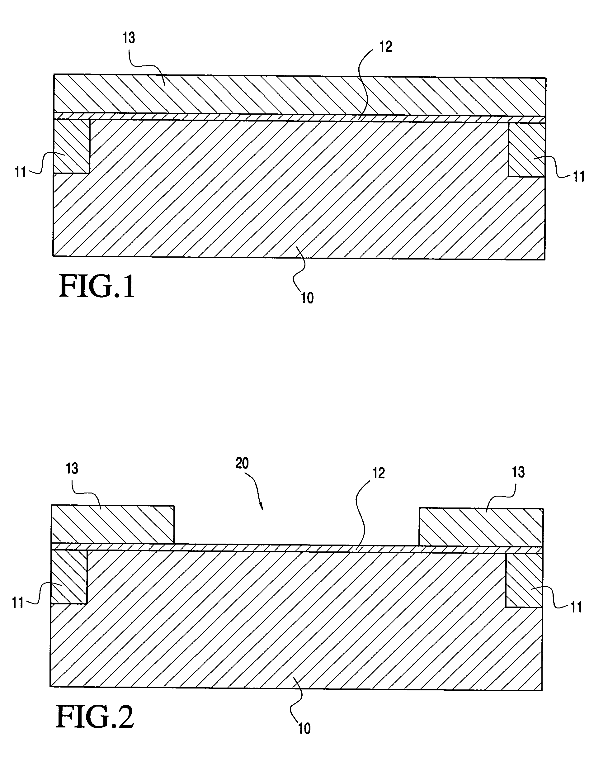
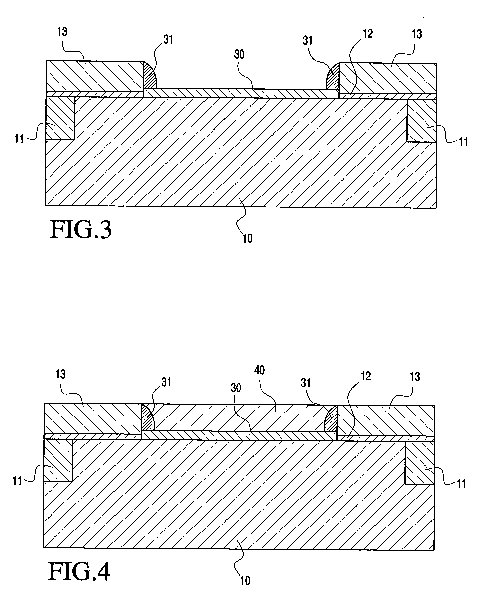
[0032]An exemplary method of fabricating the inventive resettable fuse device is illustrated in FIGS. 1-7, and will help in understanding the operation of the device, discussed be...


PUM


Abstract

A resettable fuse device is fabricated on one surface of a semiconductor substrate (10) and includes: a gate region (20) having first and second ends; a source node (81) formed in proximity to the first end of the gate region; an extension region (52) formed to connect the source node to the first end of the gate region; and a drain node (80) formed in proximity to the second end of the gate region and separated from the gate region by a distance (D) such that upon application of a predetermined bias voltage to the drain node a connection between the drain node and the second end of the gate region is completed by junction depletion. A gate dielectric (30) and a gate electrode (40) are formed over the gate region. Current flows between the source node and the drain node when the predetermined bias is applied to both the drain node and the gate electrode.

Description

BACKGROUND OF THE INVENTION[0001]1. Field of the Invention[0002]The invention relates to a simple resettable fuse device that can be used in digital and analog integrated circuits for the adding or removing circuit elements on a dynamic basis.[0003]2. Background Information[0004]Fuse devices are useful in integrated circuits for disconnecting or disabling failed circuit elements. In a RAM cell array, for example, it is well known in the art to fabricate on the silicon chip miniature metallic fuses that are in series with the memory data lines. If in the process of testing during the manufacturing cycle, a defective memory location is detected, the appropriate hard fuse can be severed, rendering the bad location inoperable. While simple to fabricate, a disadvantage of the hard fuse is that the change is permanent. Moreover, once the RAM cell array is sealed after testing, any further failures of memory locations cannot be cannot corrected by severing fuse links, and the entire device...

Claims


Application Information

Patent Timeline
Patent Type & Authority Patents(United States)
IPC IPC(8): H01L29/00H01L21/44
CPCH01L23/5256H01L2924/0002H01L2924/00
Inventor ABADEER, WAGDI WILLIAMFIFIELD, JOHN ATKINSONGAUTHIER, JR., ROBERT J.TONTI, WILLIAM ROBERT
Owner GOOGLE LLC
Learn More