[0020]Like reference numerals refer to corresponding parts throughout the drawings.
DETAILED DESCRIPTION OF THE INVENTION
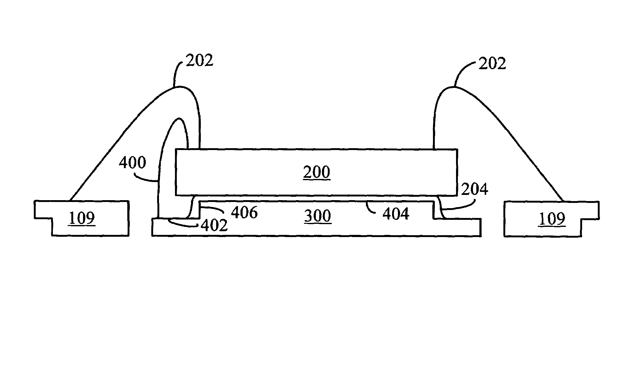
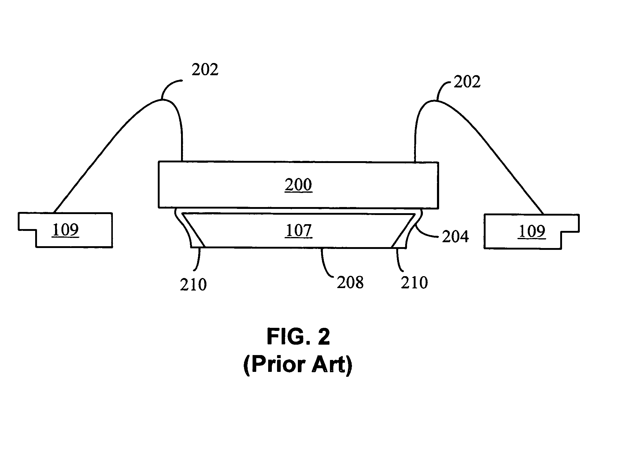
[0021]In one embodiment, a die attach pad having a peripheral ledge for collecting any adhesive that may overflow from the upper surface of the die attach pad is described. FIG. 3 illustrates a cross-section view of an LLP package constructed in accordance with an embodiment of the present invention. A die attach pad 300 has a die support surface 302 and a peripheral ledge 304. When the die 200 is affixed to the die attach pad 300, a portion of the adhesive 204 may overflow from the upper surface 302, where it accumulates on the peripheral ledge 304 instead of flowing down toward the bottom surface 306. In this manner, the peripheral ledge 304 collects excess adhesive 204 that spills over from the upper surface 302, preventing it from flowing down off of the die attach pad 300 and creating undesired conductive areas on the outer surface of the encapsulant 312.
[0022]It can be observed that creating the ledge 304 can generally produce an upper support surface 302 having a smaller area than that of the bottom surface 306. This results in a smaller area of bonding between the upper surface 302 and the die 200. As the stresses caused by phenomena such as thermal expansion and moisture absorption are proportional to the size of the die attach area, the die attach pad 300 also helps reduce these stresses, and thus the risk of delamination. Specifically, by reducing the stresses that can build up at the interfaces between the adhesive 204 and die 200 and die attach pad 300, the risk of delamination between the adhesive 204 and die 200, or between the adhesive 204 and die attach pad 300, is reduced.
[0023]It should also be observed that the peripheral ledges 304 can be incorporated into current lead-frame strips to facilitate IC manufacturing processes. FIGS. 4A–C illustrate successively more detailed views of a lead-frame strip having die attach pads constructed as those in FIG. 3. Similar to FIGS. 1A–C, FIGS. 4A–C show a lead-frame strip or panel 351 with two-dimensional arrays 353 of device areas 355. Each device area 355 in turn includes a die attach pad 357 and a plurality of contacts 359 connected by fine tie bars 361. As discussed above, the die attach pad 357 includes a peripheral ledge along all four of its sides, forming a die support surface 363. Such a lead-frame 351 can therefore be employed in connection with known processes to produce packaged ICs incorporating advantages of the invention.
[0024]In the embodiment illustrated in FIGS. 4A–C, the peripheral ledge is provided on all four sides of the die attach pad. However, in alternative embodiments, the ledge can be provided on less than all of the sides of the die attach pad. It should be appreciated that the invention is not limited to the geometry of the peripheral ledge shown in FIGS. 3 and 4A–C. That is, while the peripheral ledge 304 is shown as a relatively flat ledge or area, the geometry of the ledge need not be so limited. Rather, the peripheral ledges of any geometry suitable for retaining an amount of adhesive 204 may be used. In this manner, the invention encompasses peripheral ledges 304 that are not flat, but rather are angled or curved.
[0025]In the embodiment illustrated in FIG. 3, the invention is implemented in the context of an LLP type package. However, it should be appreciated that the described ledges may be useful in a wide variety of other package designs as well. It should be apparent that the described ledge structure is particularly useful in packages having an exposed die attach pad such as the LLP lead-frame shown in FIG. 3. However, the invention is not limited to such embodiments. Rather, the described ledges may also be used in packages having encapsulated die attach pads.
[0026]Similarly, the invention is not limited to the retaining of adhesive simply to prevent electrically conductive areas 210 on the outer surfaces of packaged ICs. Rather, the invention can also be employed to retain adhesive so as to create more dependable and reliable down bonds. FIG. 5 illustrates a cross-section view of a prior art lead-frame in which the die is down bonded to the die attach pad. In such a configuration, the die 200 is wire bonded with bond wires 202 extending to the contacts 109 as in FIG. 2, but is also down bonded to the die attach pad 300 with a down bond 400. As can be seen, attaching the die 200 to the die attach pad 300 risks displacing an amount of the adhesive 204 to the area of the down bond 400. This not only risks compromising the integrity of the electrical connection between the down bond 400 and die attach pad 300, but also increases the risk of delamination between the adhesive 204, die attach pad 300, and down bond 400.
[0027]By employing a peripheral area to retain adhesive 204, the invention can be employed to reduce the risk of adhesive flowing to the area of the down bond 400, and thus the risk of delamination. FIG. 6 illustrates a lead-frame and down-bonded die configured in accordance with an embodiment of the present invention. In this embodiment, the die attach pad 30 has a peripheral area 402 to which the down bond 400 is affixed. The peripheral area 402 creates additional space for excess adhesive 204. In this manner, adhesive 204 that flows from the upper surface 404 of the die attach pad 300 is retained relatively close to the outer edge 406, and away from the down bond 400. The presence of the peripheral ledge 402 thus retains a portion of the adhesive 204, inhibiting any flow toward the down bond 400.
[0028]The fabrication of lead-frames such as those shown in FIGS. 3 and 6 is accomplished by known process steps. Namely, die attach pads 300 are fabricated according to known steps, and the peripheral areas 304, 402 are carved out according to known masking and etching processes. It is often convenient to fabricate the peripheral areas 304, 402 by known half-etching processes, however the invention encompasses any process for carving out peripheral areas 304, 402, such as stamping. A lead-frame panel can thus be fabricated in which each device area includes these peripheral portions 304, 402. Once the lead-frame is fabricated, semiconductor dice can be attached and packaged. An amount of adhesive 204 is then applied to each die attach pad 300, and dice 300 are affixed to the die attach pad 300. If any excess adhesive 204 flows off the upper surfaces 302, 404 of the die attach pads 300, it is retained on the peripheral portions 304, 402, and prevented from either flowing into the area of down bonds 400, or off the die attach pads 300 completely.
[0029]Once the dice have been attached and properly wirebonded and/or downbonded, encapsulant can be applied to form a completed IC package. As the peripheral areas 304, 402 have caught and retained any excess adhesive 204 that has flowed from the die support surfaces 302, 404, no unwanted conductive areas such as conductive areas 201 will exist on the outer surface of the encapsulant. Specifically, in the LLP context, it can be seen that the bottom surfaces 306, 310 of the die attach pad 300 and contacts 109 remain the only exposed and electrically conductive surfaces.
[0030]The foregoing description, for purposes of explanation, used specific nomenclature to provide a thorough understanding of the invention. However, it will be apparent to one skilled in the art that the specific details are not required in order to practice the invention. Thus, the foregoing descriptions of specific embodiments of the present invention are presented for purposes of illustration and description. They are not intended to be exhaustive or to limit the invention to the precise forms disclosed. It should be apparent that many modifications and variations are possible in view of the above teachings. For example, as described above, the invention is not limited to the LLP context, but instead can be utilized to retain adhesive in many different packages. Similarly, the invention is not limited to the half-etching of flat ledges located near the periphery of a die attach pad, but in fact includes the fabrication of any die attach pad structure suitable for retaining an amount of die attach adhesive. The embodiments were chosen and described in order to best explain the principles of the invention and its practical applications, to thereby enable others skilled in the art to best utilize the invention and various embodiments with various modifications as are suited to the particular use contemplated. It is intended that the scope of the invention be defined by the following claims and their equivalents.