Data output circuit, data output method, and semiconductor memory device

a data output and data technology, applied in the field of data output circuits, can solve the problems of increasing the operation speed of the semiconductor device, affecting the accuracy of the data signal, and the misoperation of other semiconductor devices receiving the data signal dq, etc., and achieve the effect of accurate equalization

Inactive Publication Date: 2007-06-05
SAMSUNG ELECTRONICS CO LTD
View PDF17 Cites 5 Cited by
  • Summary
  • Abstract
  • Description
  • Claims
  • Application Information

AI Technical Summary

Benefits of technology

[0028]The present invention provides a data output circuit capable of automatically or more accurately equalizing a delay time of a data strobe signal replication unit and a delay time of a data strobe signal output unit.
[0029]The present invention also provides a data output method capable of automatically or more accurately equalizing a delay time of a data strobe signal replication unit and a delay time of a data strobe signal output unit.
[0030]The present invention also provides a semiconductor memory device capable of automatically or more accurately equalizing a delay time of a data strobe signal replication unit and a delay time of a data strobe signal output unit.

Problems solved by technology

As a result, there may occur mis-operation in other semiconductor devices receiving the data signal DQ in accordance with the external clock signal CLK.
The aforementioned problem also occurs in a case where the other semiconductor device senses the data signal DQ at rising and falling edges of the external clock signal CLK.
The problem becomes more serious as the operation speed of the semiconductor device increases.
However, it is generally difficult to obtain an accurate modeling of the data strobe signal output unit 20.
In addition, a large amount of time is required for performing the simulation using the modeling.
In other words, the aforementioned conventional method has shortcomings in that it is difficult to accurately determine the delay time tREP of the data strobe signal replication unit 30 and too much time is required for an accurate determination of the delay time.
In addition, although the modeling error and the process-oriented error can be corrected at the package level, it is impossible to adjust a difference between a plurality of packages fabricated from a single, common wafer.
Therefore, in the conventional data output circuit, there is a high probability of errors occurring between the delay time tREP of the data strobe signal replication unit 30 and the delay time tCLK of the data strobe signal output unit 20.
As a result, a semiconductor device receiving the output data may receive invalid data.
These problems become more serious as the operation speed of the semiconductor device increases.

Method used


Image

  • Data output circuit, data output method, and semiconductor memory device
  • Data output circuit, data output method, and semiconductor memory device
  • Data output circuit, data output method, and semiconductor memory device

Examples


first embodiment

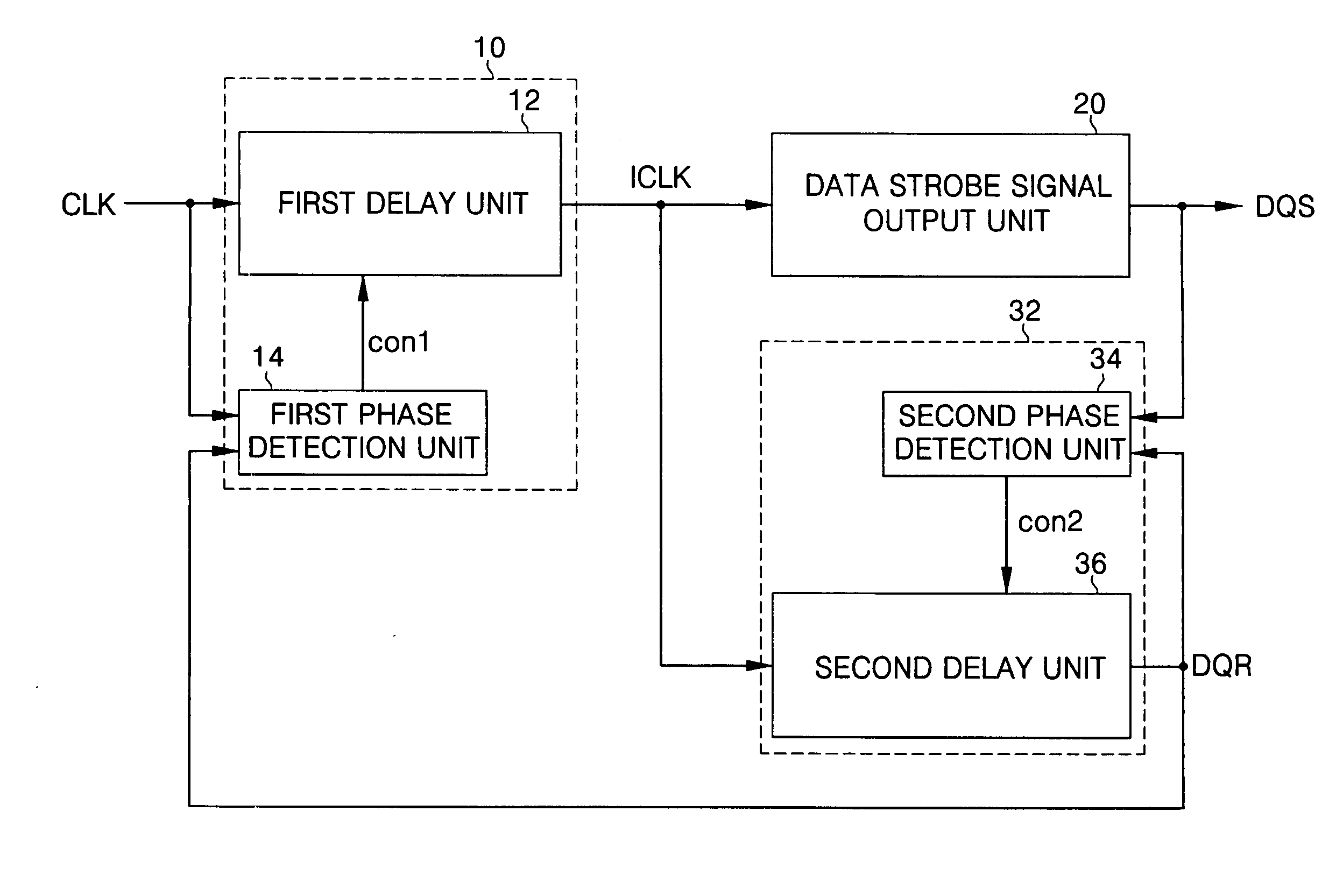
[0062]FIG. 5 is a block diagram showing a second delay unit 36 of a data strobe signal replication unit 32 of the data output circuit according to the present invention shown in FIG. 4. The second delay unit 36 comprises a shift register 361 and a delay cell array 362.

[0063]Now, functions of the blocks shown in FIG. 5 will be described.

[0064]The shift register 361 outputs a delay time adjustment signal in response to a second control signal con2 output from the second phase detection unit 34. More specifically, the shift register 361 outputs a high level output signal through one of four output ports Q1˜Q4 and low level output signals through the other ports. The port for outputting the high level output signal is selected by the second control signal con2.

[0065]The delay cell array 362 comprises four delay cells IV1˜IV4 and eight NAND gates ND1˜ND8. The delay cell array 362 selects some of the delay cells in response to the delay time adjustment signal and delays the internal clock...

second embodiment

[0070]FIG. 6 is a block diagram showing a second delay unit 36 of a data strobe signal replication unit 32 of the data output circuit according to the present invention shown in FIG. 4. The second delay unit 36 comprises a counter 363, a bias output unit 364, and a delay cell 365.

[0071]Now, the functions of the blocks shown in FIG. 6 will be described.

[0072]The counter 363 outputs the delay time adjustment signal in response to the second control signal con2 output from the second phase detection unit 34. More specifically, the counter 363 increases or decreases a value of the delay time adjustment signal having a binary code format or a thermometer code format in response to the second control signal con2.

[0073]The bias output unit 364 changes a bias current output in response to the delay time adjustment signal. More specifically, NMOS transistors N1˜N4 constituting the bias output unit 364 are turned on or off in response to bits of the delay time adjustment signal. It can be und...


PUM


Abstract

In a data output circuit, a data output method, and a semiconductor memory device, the data output circuit includes: an internal clock generation unit that delays an external clock signal by a first delay time to output an internal clock signal in response to the external clock signal and a replica data strobe signal; a data strobe signal output unit that outputs a data strobe signal in response to the internal clock signal; and a data strobe signal replication unit that delays the internal clock signal by a second delay time to output the replica data strobe signal and changing the second delay time in response to the data strobe signal and the replica data strobe signal. Accordingly, it is possible to save time and effort required for setting a delay time of a data strobe signal replication unit. In addition, it is possible to correct differences between packages of the delay time of the data strobe signal output unit.

Description

CROSS-REFERENCE TO RELATED PATENT APPLICATION[0001]This application claims the benefit of Korean Patent Application No. 10-2004-0112332, filed on Dec. 24, 2004, in the Korean Intellectual Property Office, the disclosure of which is incorporated herein in its entirety by reference.BACKGROUND OF THE INVENTION[0002]1. Field of the Invention[0003]The present invention relates to a data output circuit, and more particularly, to a data output circuit employing a delay locked loop used in a synchronous semiconductor device.[0004]2. Description of the Related Art[0005]In general, synchronous semiconductor devices output data in synchronization with an external clock signal. For the synchronization, delay locked loops (DLLs) including a delay unit and a phase detection unit have been widely used. The delay locked loop delays the external clock signal by a predetermined time period to generate an internal clock signal. More specifically, the phase detection unit detects a phase difference bet...

Claims


Application Information

Patent Timeline
Patent Type & Authority Patents(United States)
IPC IPC(8): G11C7/00
CPCG11C7/1051G11C7/1057G11C7/1066G11C7/22G11C7/222G11C7/10
Inventor LEE, JAE-HYUNG
Owner SAMSUNG ELECTRONICS CO LTD
Why Eureka
Try Eureka