System and method for manufacturing an out of plane integrated circuit inductor

a manufacturing method and integrated circuit technology, applied in the direction of inductances, basic electric elements, electrical appliances, etc., can solve the problems of lossy eddy current, degrade the quality factor (q) of the inductor, and art methods for forming these types of out of plane inductors, so as to achieve the effect of reducing manufacturing steps and avoiding lossy eddy curren

Active Publication Date: 2007-06-12
NAT SEMICON CORP
View PDF23 Cites 27 Cited by
  • Summary
  • Abstract
  • Description
  • Claims
  • Application Information

AI Technical Summary

Benefits of technology

[0012]It is also an object of the present invention to provide a system and method for manufacturing a relatively inexpensive and simple out of plane integrated circuit inductor.
[0013]It is yet another object of the present invention to provide a system and method for manufacturing a reliable out of plane integrated circuit inductor that requires a minimum of manufacturing steps.

Problems solved by technology

Magnetic flux in the substrate induces lossy eddy currents and degrades the quality factor (Q) of the inductor.
The prior art methods for forming these types of out of plane inductors have significant drawbacks.
The prior art methods tend to be relatively expensive, require numerous and complex manufacturing steps, and have questionable controllability.
In addition, some of the prior art manufacturing methods require considerable time to perform.

Method used


Image

  • System and method for manufacturing an out of plane integrated circuit inductor
  • System and method for manufacturing an out of plane integrated circuit inductor
  • System and method for manufacturing an out of plane integrated circuit inductor

Examples


Embodiment Construction

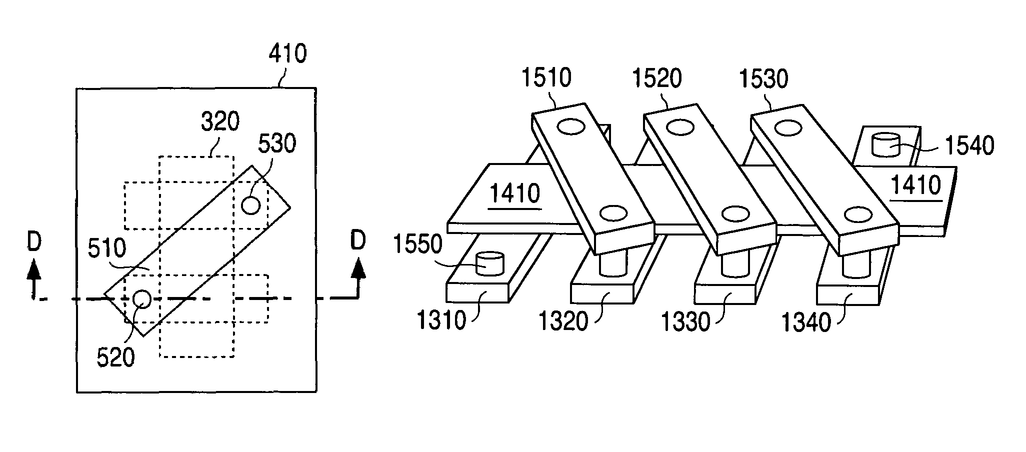
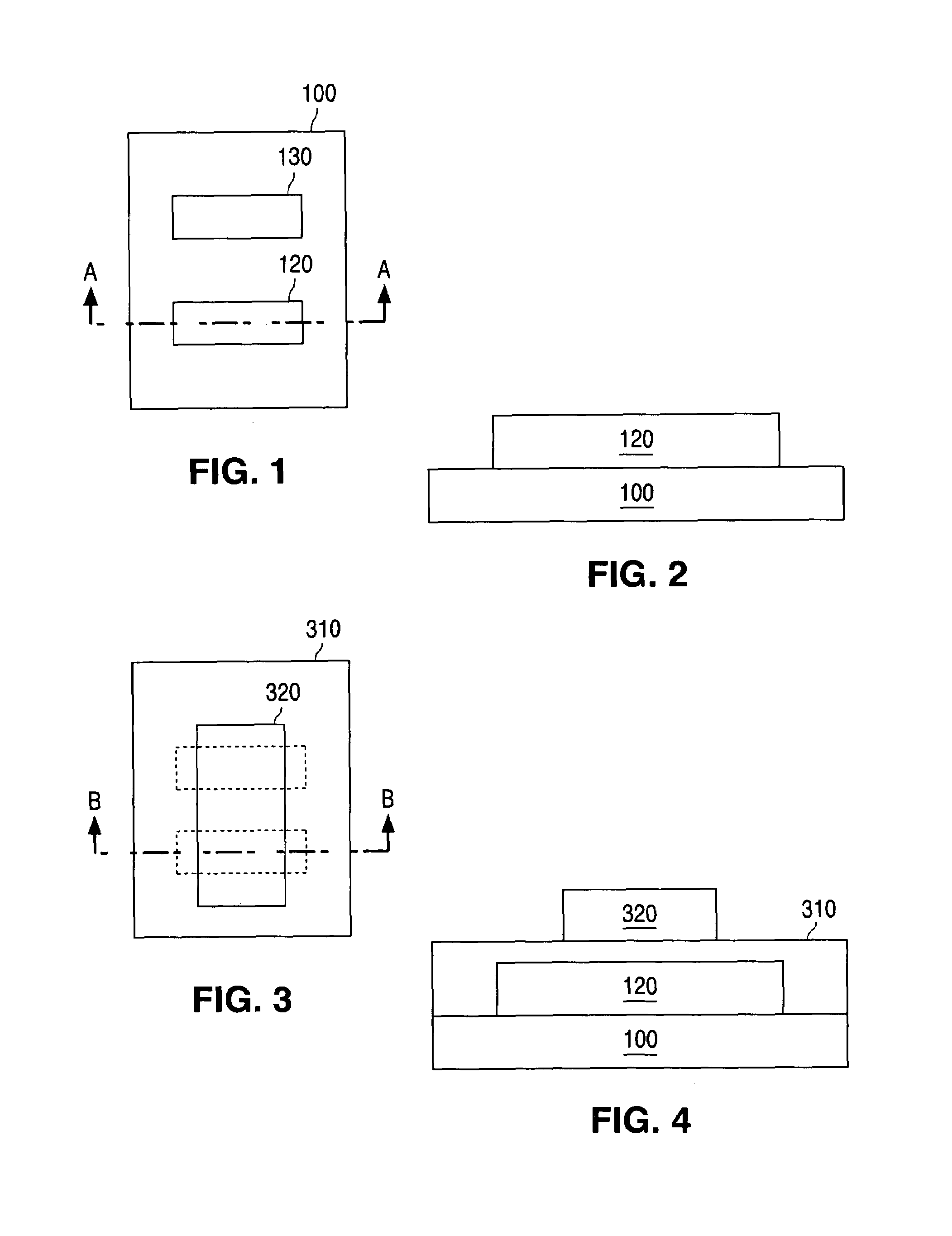
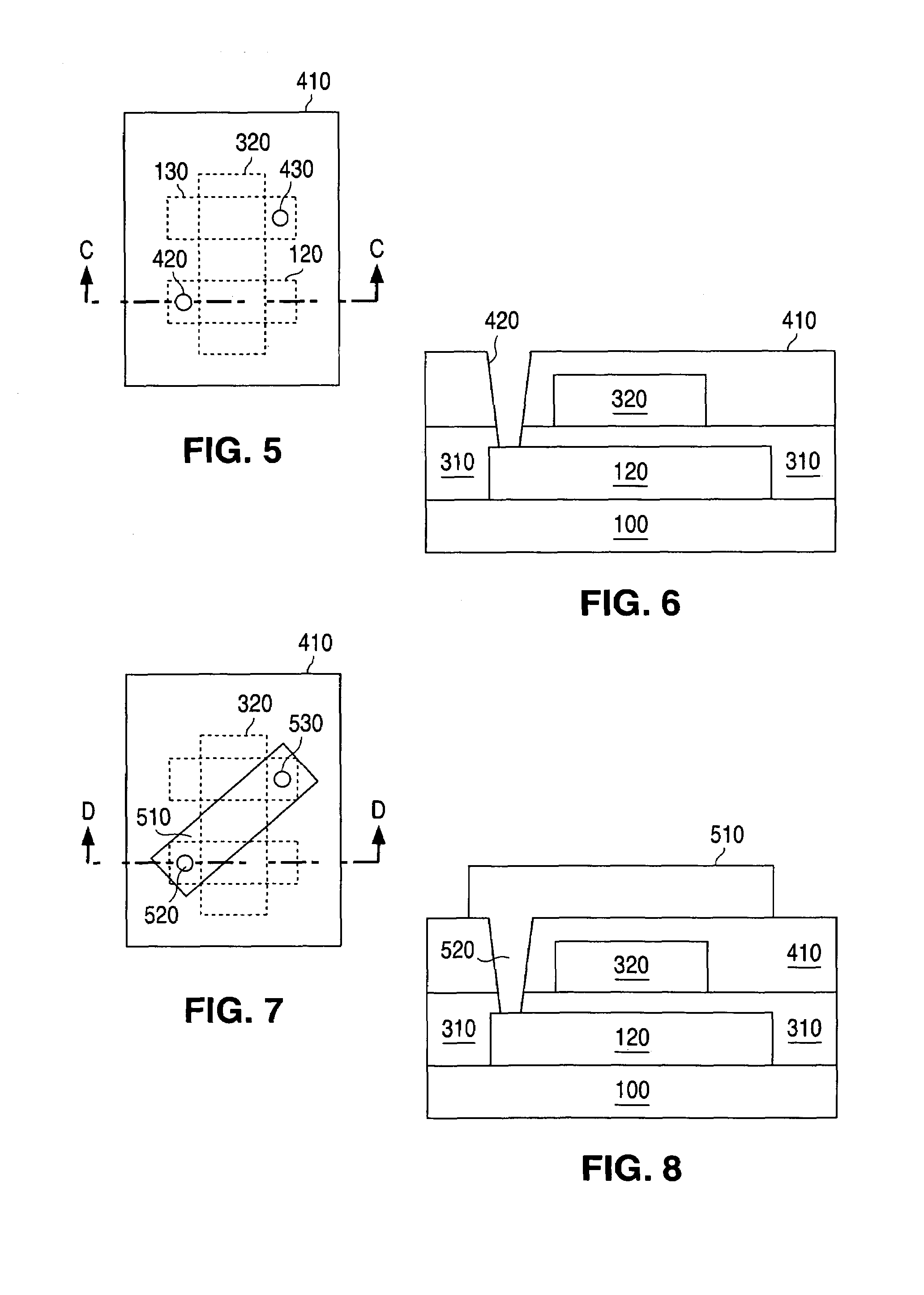
[0036]FIGS. 1 through 17, discussed below, and the various embodiments used to describe the principles of the present invention in this patent document are by way of illustration only and should not be construed in any way to limit the scope of the invention. Those skilled in the art will understand that the principles of the present invention may be implemented in any type of suitably arranged integrated circuit.

[0037]To simplify the drawings the reference numerals from previous drawings may sometimes not be repeated for structures that have already been identified.

[0038]An advantageous embodiment of the inductor coil of the present invention will be described that comprises a plurality of parallel metal bars formed on a substrate. It is understood that the location of the plurality of parallel metal bars on an underlying substrate is merely an example and that the plurality of parallel metal bars may be part of any suitable metal layer of an integrated circuit. That is, in an alte...


PUM


Abstract

A system and method is described for manufacturing an out of plane integrated circuit inductor. A plurality of parallel metal bars are formed on a substrate and covered with a first passivation layer. A ferromagnetic core is then deposited over the first passivation layer with its length perpendicular to the plurality of parallel metal bars. A second passivation layer is deposited over the ferromagnetic core and vias are etched through the passivation layers to the alternate ends of the underlying parallel metal bars. A plurality of cross connection metal bars are then formed on the second passivation layer with vertical portions that fill the vias and connect the alternate ends of the plurality of parallel metal bars to form an inductor coil. A third passivation layer is then deposited over the cross connection metal bars.

Description

TECHNICAL FIELD OF THE INVENTION[0001]The present invention is generally directed to manufacturing technology for semiconductor devices and, in particular, to a system and method for manufacturing an out of plane integrated circuit inductor.BACKGROUND OF THE INVENTION[0002]Some types of prior art integrated circuit inductors have coils that lie in a plane that is parallel to the plane of an underlying substrate. The axis of the coils in these “in plane” inductors is perpendicular to the plane of the underlying substrate. This arrangement causes most of the magnetic flux of the inductor to penetrate into the substrate. Magnetic flux in the substrate induces lossy eddy currents and degrades the quality factor (Q) of the inductor.[0003]To solve this problem various types of prior art “out of plane” integrated circuit inductors have been developed. One type of prior art “out of plane” inductor comprises three dimensional micro-coils that are fabricated on a planar substrate. The three d...

Claims


Application Information

Patent Timeline
Patent Type & Authority Patents(United States)
IPC IPC(8): H01L21/4763H01L21/44
CPCH01L28/10
Inventor DRIZLIKH, SERGEITHIBEAULT, TODD
Owner NAT SEMICON CORP
Why Eureka
Try Eureka