
Driver circuit

Active Publication Date: 2007-06-12
TEXAS INSTR INC
View PDF9 Cites 6 Cited by
  • Summary
  • Abstract
  • Description
  • Claims
  • Application Information

AI Technical Summary

Benefits of technology

[0008]Additional circuitry (e.g., a filter) may be coupled to the input supply node to mitigate noise from being injected from the input supply node to an output terminal that provides a regulated output based on the first and second input signals. Biasing can also be implemented to regulate current through the second and third transistors when operating in a conductive state. The driver circuit can be employed to drive a high voltage transistor having its control input connected to the output node, such as for connecting the input supply node with an output terminal. The driver circuit also mitigates cross-regulation at the input supply node, such as when more than one load or other device is coupled to receive power via the input supply node.

Problems solved by technology

When voltage at the source of output PMOS device 2 changes in such a manner, there tends to be leakage across the PMOS device 2.
This leakage can result in cross regulation, such as when multiple power devices are driving respective loads from the same supply 11.
The high impedance at the node 12 thus reduces performance of the driver for a variety of applications.

Method used


Image

  • Driver circuit
  • Driver circuit
  • Driver circuit

Examples


Embodiment Construction

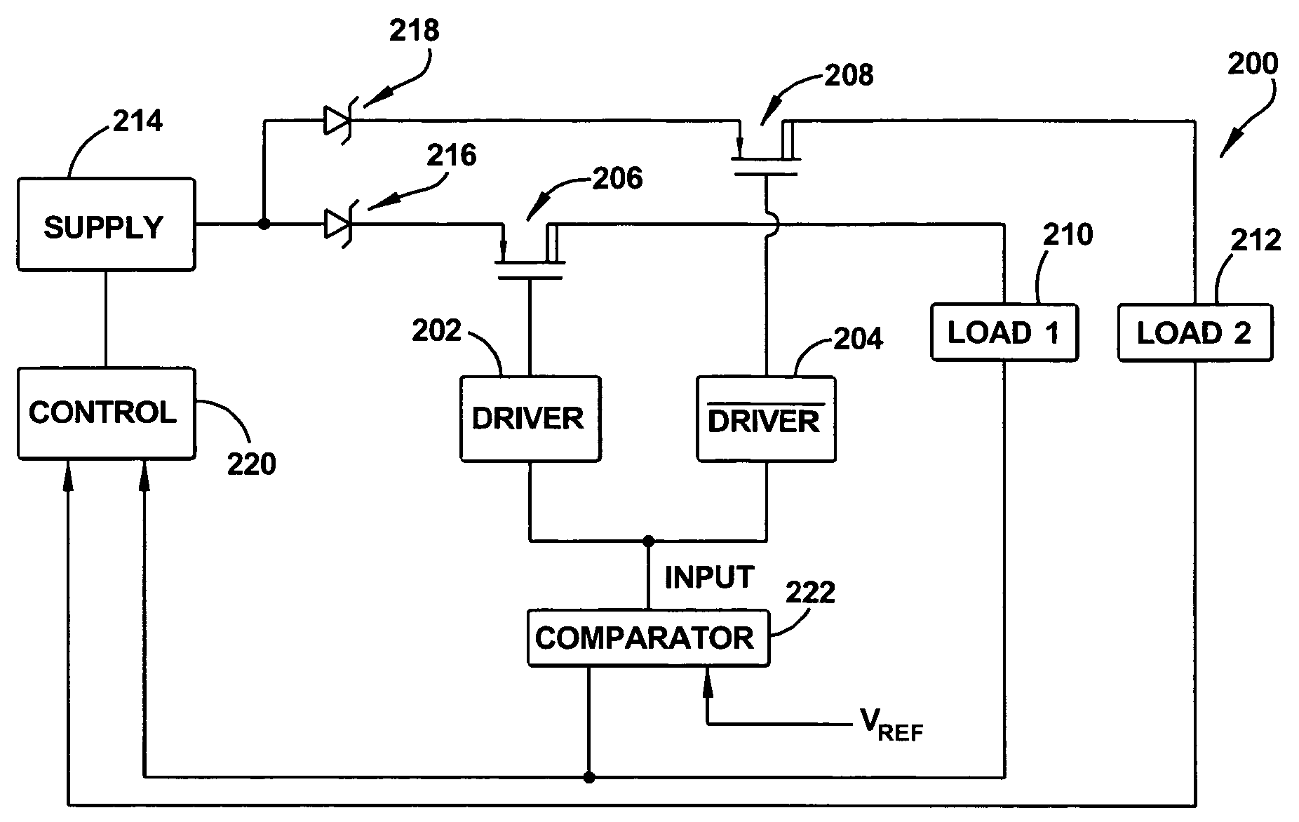
[0014]The present invention relates to a driver (or buffer) circuit that can be utilized to drive a high-voltage switch device, such as a PMOS or NMOS device, according to an aspect of the present invention. The driver circuit affords voltage protection of an output switch device as well as a reasonable amount of current consumption. Additionally, the driver circuit can provide a fast dynamic response to mitigate noise injection from the supply terminal of an associated power supply. Additionally, the driver circuit can mitigate leakage and cross regulation through an output switch device that is being driven.

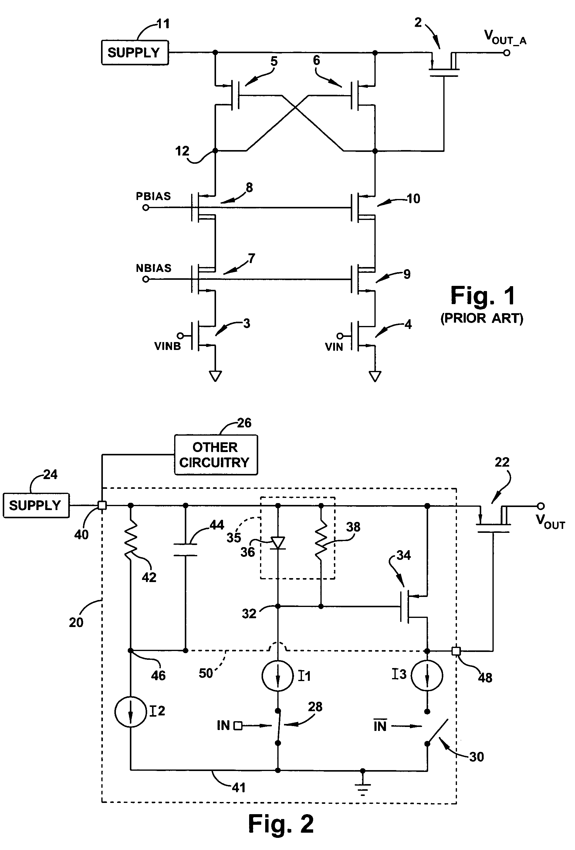
[0015]FIG. 2 depicts a high-level schematic diagram of a driver circuit 20 that can be implemented according to an aspect of the present invention. The driver circuit 20 is connected to drive an output power switch device, represented in FIG. 2 as a PMOS device 22. The driver circuit 20, however, is not limited in its application to driving a given type of transistor device.

[00...


PUM


Abstract

A driver circuit includes a first transistor coupled between an input supply node and an output node. The first transistor operates in one of a conductive state to couple the output node with the input supply node and non-conductive state according to cooperative operation of a second transistor and a third transistor. The second transistor is coupled to provide a control input to drive the first transistor to the conductive state thereof in response a first input signal provided at a control input of the second transistor. The third transistor is coupled to provide an output at the output node in response to a second input signal provided at a control input of the third transistor, the first and second input signals being out of phase with each other. Circuitry is coupled between the input supply node and the control input of the first transistor to provide reduced impedance at the control input of the first transistor according to operation of the second transistor.

Description

TECHNICAL FIELD[0001]The present invention relates to electrical circuits and, more particularly, to a driver circuit.BACKGROUND[0002]Various circuits have been developed, as drivers or buffers, for use in driving high voltage devices. For instance, such drivers or buffers can be formed of low-voltage electronic circuitry, to drive high-voltage power devices, such as power metal oxide semiconductor field effect transistors (MOSFETs), insulated gate bipolar transistor devices (IGBTs), gate controlled thyristors, and the like.[0003]The low-voltage circuitry can be coupled to apply appropriate voltages to the gate or control terminal of the power device to turn on or turn off the power device. When the power device is an N-channel metal oxide semiconductor field effect transistor (NMOSFET, also referred to as an NFET or NMOS device), the device is turned on by applying a high voltage to the gate of the power switch and turned off by applying a low voltage to the gate. In contrast, if t...

Claims


Application Information

Patent Timeline
IPC IPC(8): H03K19/0175
CPCH03K17/04206H03K17/0822H03K17/165
Inventor HOON, SIEW KUOKMALOBERTI, FRANCOCHEN, JUN
Owner TEXAS INSTR INC
Features
  • Generate Ideas
  • Intellectual Property
  • Life Sciences
  • Materials
  • Tech Scout
  • Unparalleled Data Quality
  • Higher Quality Content
  • 60% Fewer Hallucinations
Learn More