Image sensing apparatus having image signals generated from light between optical elements of an optical element array

Active Publication Date: 2007-06-19
CANON KK
View PDF16 Cites 41 Cited by
  • Summary
  • Abstract
  • Description
  • Claims
  • Application Information

AI Technical Summary

Benefits of technology

[0014]The present invention has been made in consideration of the above problems in the prior art, and has as its object to realize an

Problems solved by technology

In general, in focus detection based on such a contrast detection scheme, since evaluation function values are obtained while the position of an image sensing optical system on the optical axis is slightly moved, it requires a considerable time to perform focus adjustment until an in-focus state is obtained.
However, this scheme includes both pixels with short optical path lengths and pixels with long optical path lengths and hence is not suited to an apparatus aiming at obtaining high-quality images.
Although the image quality improves as the optical path length differences between pixels with short optical path lengths and pixels with long optical path lengths are reduced, it becomes difficult to perform direction determination in focus control.
It is therefore impossible to realize both high-speed focus control and high image quality.
In the image sensing device having the structure disclosed in U.S. Pat. No. 4,410,804, since one or two pairs of images formed by light beams passing through portions of the pupil of the image sensing optical system are output, these images have very low quality when eval

Method used


Image

  • Image sensing apparatus having image signals generated from light between optical elements of an optical element array
  • Image sensing apparatus having image signals generated from light between optical elements of an optical element array
  • Image sensing apparatus having image signals generated from light between optical elements of an optical element array

Examples


Example

First Embodiment

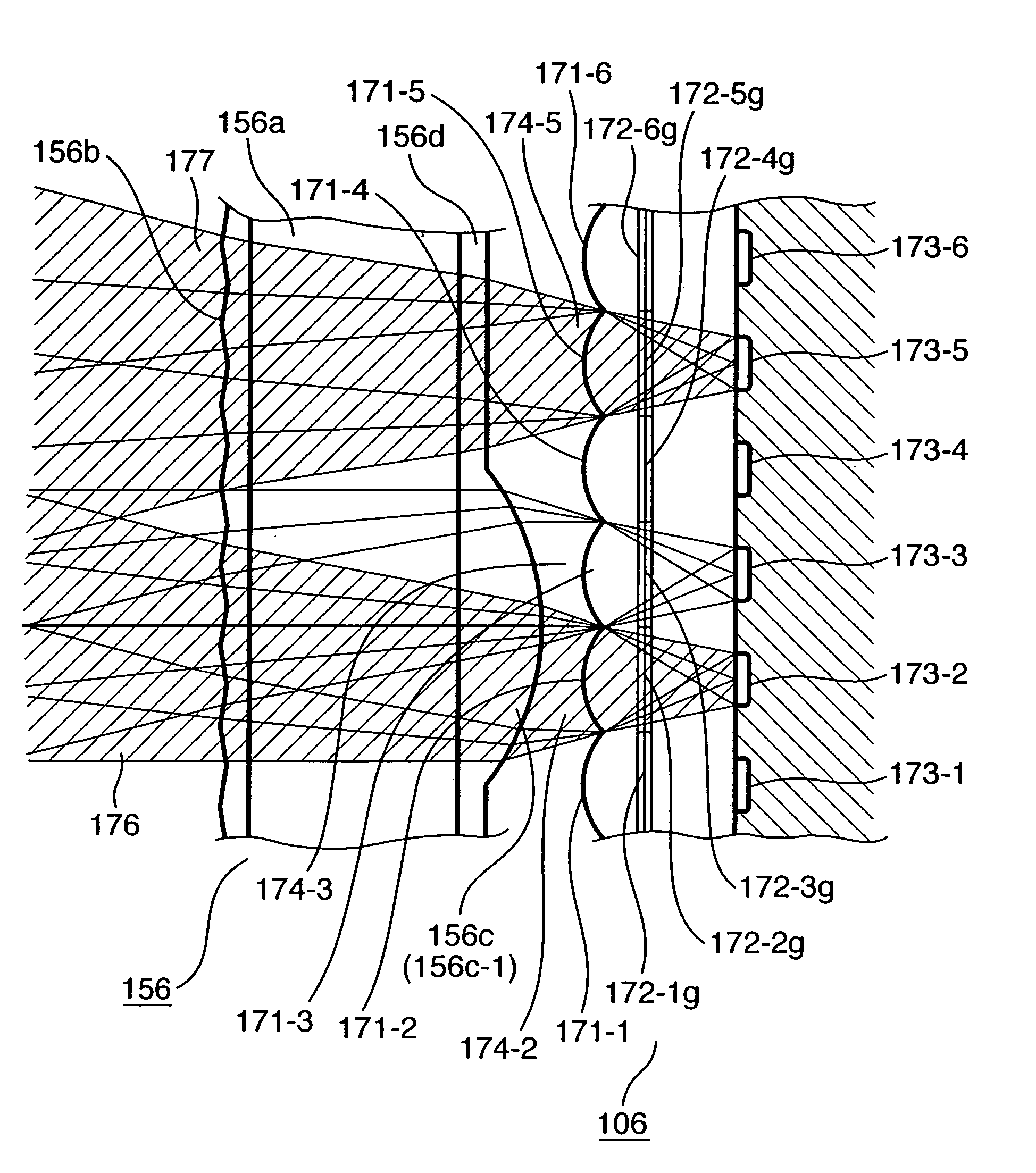
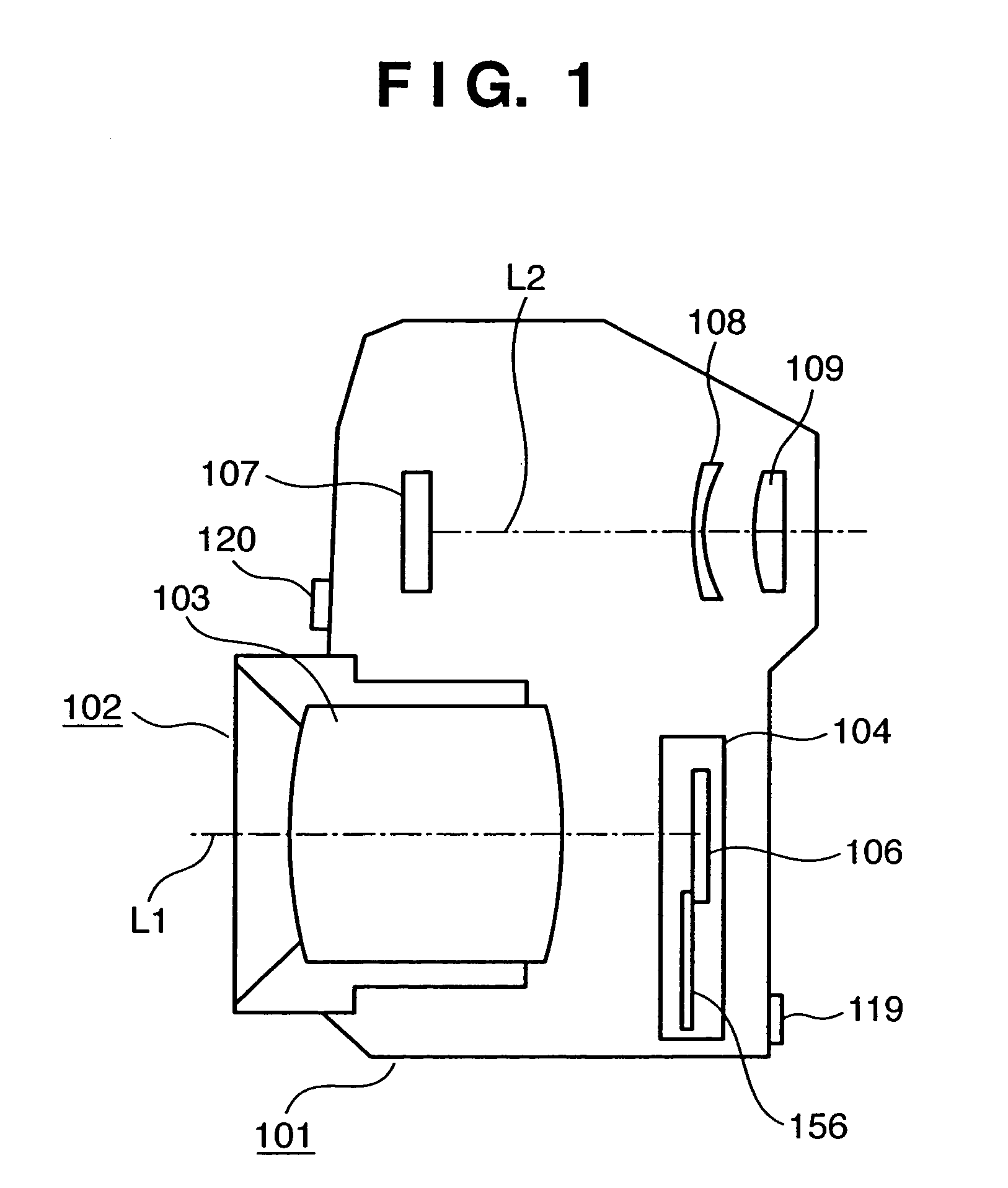
[0055]FIG. 1 is a view showing the schematic arrangement of a digital color camera which is image sensing equipment incorporating an image sensing apparatus according to the first embodiment of the present invention. This camera is a single-CCD digital color camera which uses an image sensing device such as a CCD or CMOS sensor. The camera obtains an image signal representing a moving or still image by continuously or sporadically driving the image sensing device. In this case, the image sensing device is an area sensor of a type that converts exposure light into an electrical signal for each pixel, stores electric charges corresponding to the light amount, and outputs the electric charges.

[0056]Referring to FIG. 1, reference numeral 101 denotes a camera body; and 102, a detachable photographing lens incorporating an imaging optical system 103. The photographing lens 102 is electrically and mechanically connected to the camera body 101 through a known mount. Photogra...

Example

Second Embodiment

[0141]FIGS. 12 and 13 are views showing the schematic arrangement of a digital color camera incorporating an image sensing apparatus according to the second embodiment of the present invention. FIG. 12 is a sectional view of the camera taken in the lateral direction. FIG. 13 is a front perspective view of the camera when viewed from the left side in FIG. 12. This camera is a single-CCD digital color camera which uses an image sensing device such as a CCD or CMOS sensor. The camera obtains an image signal representing a moving or still image by continuously or sporadically driving the image sensing device. In this case, the image sensing device is an area sensor of a type that converts exposed light into an electrical signal for each pixel, stores electric charges corresponding to the light amount, and outputs the electric charges.

[0142]Referring to FIG. 12, reference numeral 203 denotes an imaging optical system which has a driving mechanism (not shown) and is focus...


PUM


Abstract

It is an object of this invention to realize an image sensing apparatus which satisfies both the requirements for focus detection performance and high-resolution, high image quality. In order to achieve this object, there is provided an image sensing apparatus characterized by comprising an image sensing device having a plurality of pixels, an optical element array having a plurality of optical elements made to correspond one by one to each set of a plurality number of pixels of a plurality of pixels of the image sensing device, and a focusing device which generates, for each of the plurality of optical elements, one pair of focus detection signals in the pixels from light passing through the optical element, and performs focusing operation on the basis of focus detection signals generated in pairs for each of the optical elements.

Description

FIELD OF THE INVENTION[0001]The present invention relates to an image sensing device and, more particularly, to an image sensing apparatus having a focus detection function in addition to an image sensing function using an image sensing device.BACKGROUND OF THE INVENTION[0002]In a digital camera, in response to the pressing of the release button, an image sensing device such as a CCD or CMOS sensor is exposed to an object image for a desired period of time. The resultant image signal representing a still image of one frame is converted into a digital signal. Predetermined processing such as YC processing is then performed for the digital signal to obtain an image signal in a predetermined form. Digital image signals representing sensed images are recorded on a semiconductor memory in correspondence with the respective images. The recorded image signals are read out as needed to be displayed or converted into printable signals. Alternatively, such signals are output to a display appa...

Claims


Application Information

Patent Timeline
IPC IPC(8): G03B13/00G02B7/28G03B13/36G02B7/34H04N5/225H04N5/232H04N5/335H04N101/00
CPCH04N5/23212H04N23/672H04N25/704
Inventor SUDA, YASUO
Owner CANON KK
Why Eureka
Try Eureka