Combinatorial fabrication and high-throughput screening of optoelectronic devices

Inactive Publication Date: 2007-07-24
AERIS CAPITAL SUSTAINABLE IP
View PDF6 Cites 223 Cited by
  • Summary
  • Abstract
  • Description
  • Claims
  • Application Information

AI Technical Summary

Problems solved by technology

The disadvantages associated with the prior art are over come by systematic methods and apparatus for the rapid and parallel synthesis of novel optoelectronic devices and for the high-throughput screening of such devices for useful properties.

Method used


Image

  • Combinatorial fabrication and high-throughput screening of optoelectronic devices
  • Combinatorial fabrication and high-throughput screening of optoelectronic devices
  • Combinatorial fabrication and high-throughput screening of optoelectronic devices

Examples


Embodiment Construction

Contents

I. Glossary

II. General Overview

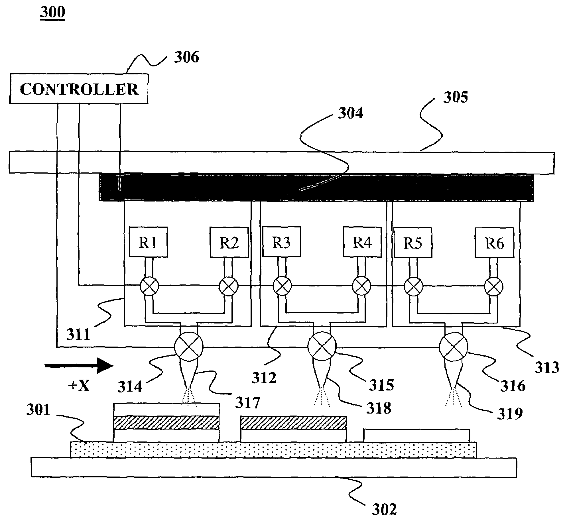
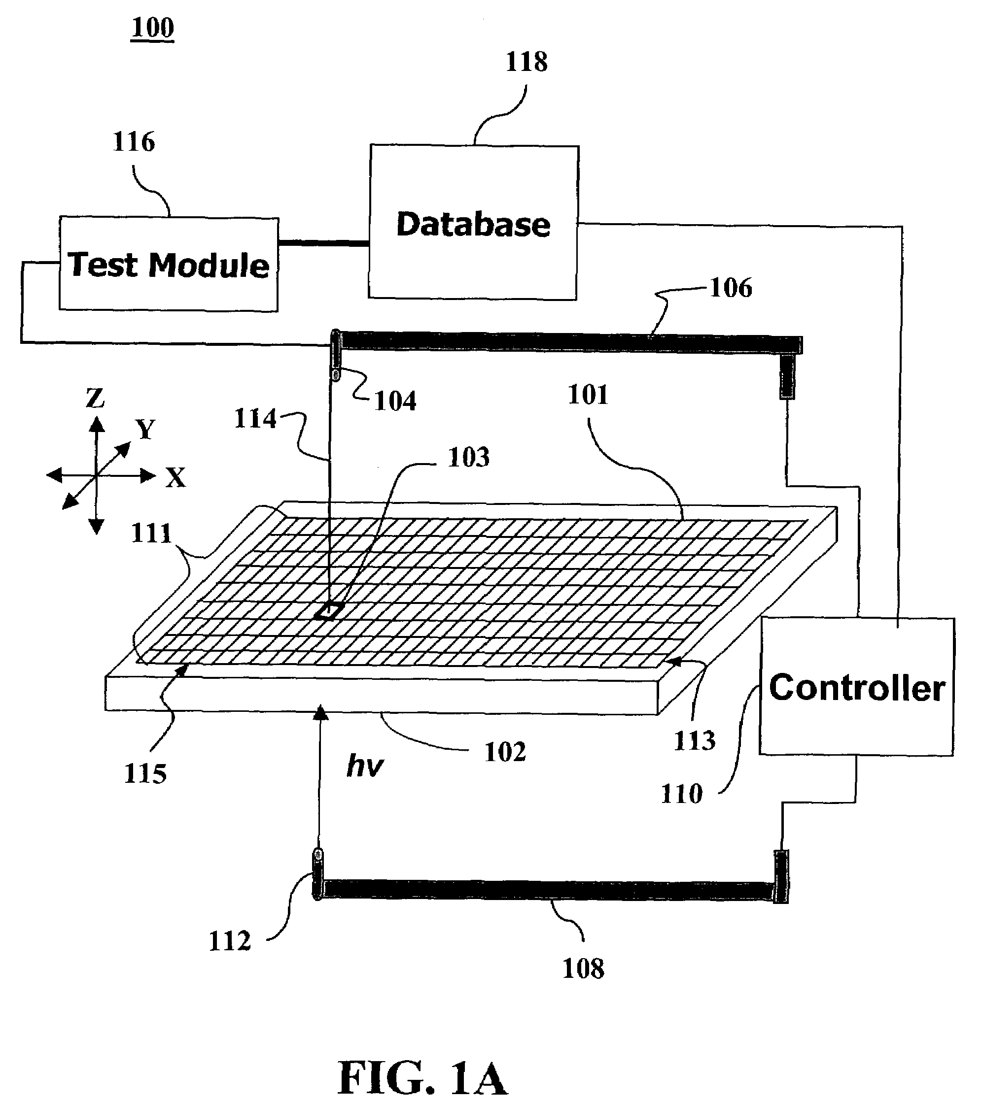
III. Fabrication of an Array of Devices

IV. Methods For Delivery Of Reactant Components

V. Moving The Dispenser With Respect To The Substrate

VI. Synthetic Routes For Reacting The Array Of Components

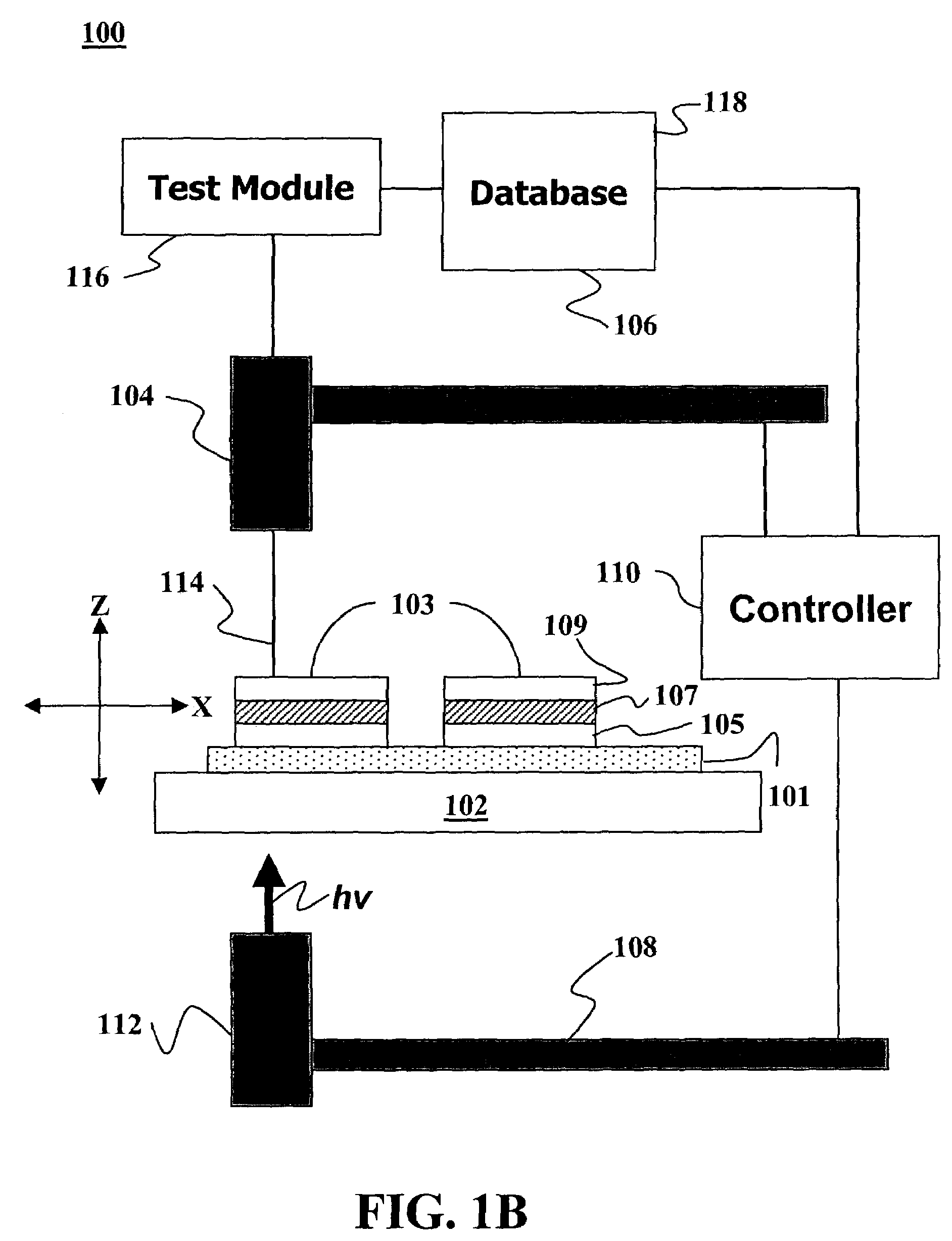
VII. Methods For Screening An Array Of Devices

VIII. Alternative Embodiments

X. Conclusion

I. GLOSSARY

[0017]The following terms are intended to have the following general meanings as they are used herein:

Combinatorial Chemistry: In general, combinatorial chemistry refers to the approach of creating vast numbers of compounds by reacting a set of starting chemicals in a variety of different possible combinations.

Device: An assembly or sub-assembly having two or more layers of material.

Optoelectronic Device: A device that interacts with radiation and electric current. Such a device could be a light-emitting device, e.g. an LED or laser, or a light absorbing device, e.g. a photodetector / counter or photovoltaic cell (solar cell).

Solar Cell: A photovoltaic devi...


PUM


Abstract

Methods and apparatus for the rapid and parallel synthesis of optoelectronic cell devices and for the high-throughput screening of such devices for useful properties are disclosed. The methods comprise the parallel synthesis of arrays of optoelectronic devices fabricated within an addressable sample-holding matrix. Each optoelectronic device is created and tested within an addressable sample-holder in the fabrication device.

Description

CROSS-REFERENCE TO RELATED APPLICATION[0001]This application claims priority to U.S. Provisional Patent Application 60 / 407,196, filed Aug. 28, 2002, the entire disclosures of which are incorporated herein by reference.FIELD OF THE INVENTION[0002]This invention generally relates to methods and apparatus for the parallel synthesis and screening of an array of optoelectronic devices, and more specifically to the combinatorial fabrication and high-throughput testing of optoelectronic devices.BACKGROUND OF THE INVENTION[0003]To optimize the efficiency and stability of optoelectronic devices, it is necessary to fabricate devices composed of specific materials and in particular architectural arrangements. The discovery of new materials and structures with novel chemical, optical, electronic, and physical properties can lead to the development of new and useful solar cell devices optimized for particular structures and / or functions[0004]Given the large number of potentially useful materials...

Claims


Application Information

Patent Timeline
Patent Type & Authority Patents(United States)
IPC IPC(8): B05D5/06
CPCG01R31/307H01L51/0004H01L51/0005H01L27/307H01S5/0014Y02E10/549H10K39/32H10K71/13H10K71/135
Inventor SAGER, BRIAN M.ROSCHEISEN, MARTIN R.PETRITSCH, KLAUS
Owner AERIS CAPITAL SUSTAINABLE IP
Why Eureka
Try Eureka