Voltage regulator with improved power supply rejection ratio characteristics and narrow response band

a voltage regulator and power supply rejection technology, applied in the field of voltage regulators, can solve the problems of high frequency noise at the output terminal, inability to compensate for negative feedback control, and rapid degradation of psrr characteristics, and achieve the effect of improving psrr characteristics

Inactive Publication Date: 2007-07-24
RENESAS ELECTRONICS CORP
View PDF11 Cites 34 Cited by
  • Summary
  • Abstract
  • Description
  • Claims
  • Application Information

AI Technical Summary

Benefits of technology

[0010]It is an object of the present invention to provide a voltage regulator having improved PSRR characteristics while maintaining the narrow response band, and capable of being incorporated into a mobile station which needs to be small both in size and power consumption.

Problems solved by technology

However, if a high frequency noise higher than a predetermined value is applied to the power supply voltage, the PSRR characteristics deteriorate rapidly, so that such a high frequency noise cannot be compensated for by the negative feedback control.
As a result, such a high frequency noise would appear at the output terminal.
In this case, however, the response band is also broadened, so that the operation would be unstable.
Also, the former approach would increase the power consumption.
Also, since the number of differential amplifiers (operational amplifiers) is increased, the power consumption would be increased and the circuit size would be increased.

Method used


Image

  • Voltage regulator with improved power supply rejection ratio characteristics and narrow response band
  • Voltage regulator with improved power supply rejection ratio characteristics and narrow response band
  • Voltage regulator with improved power supply rejection ratio characteristics and narrow response band

Examples


first embodiment

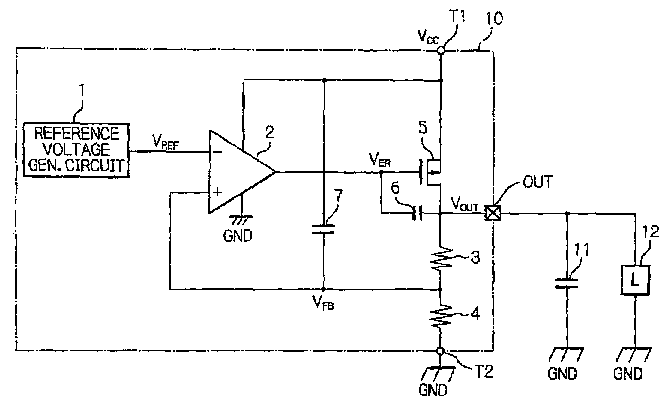
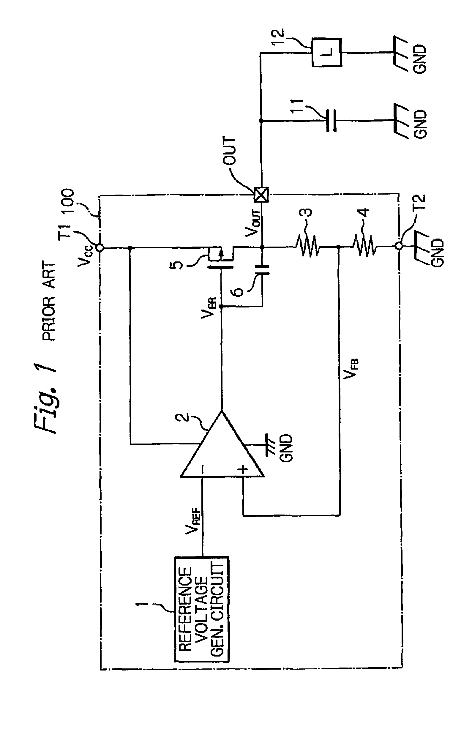
[0038]In FIG. 5, which illustrates the voltage regulator according to the present invention, a voltage regulator 10 includes a capacitor 7 in addition to the voltage regulator 100 of FIG. 1.

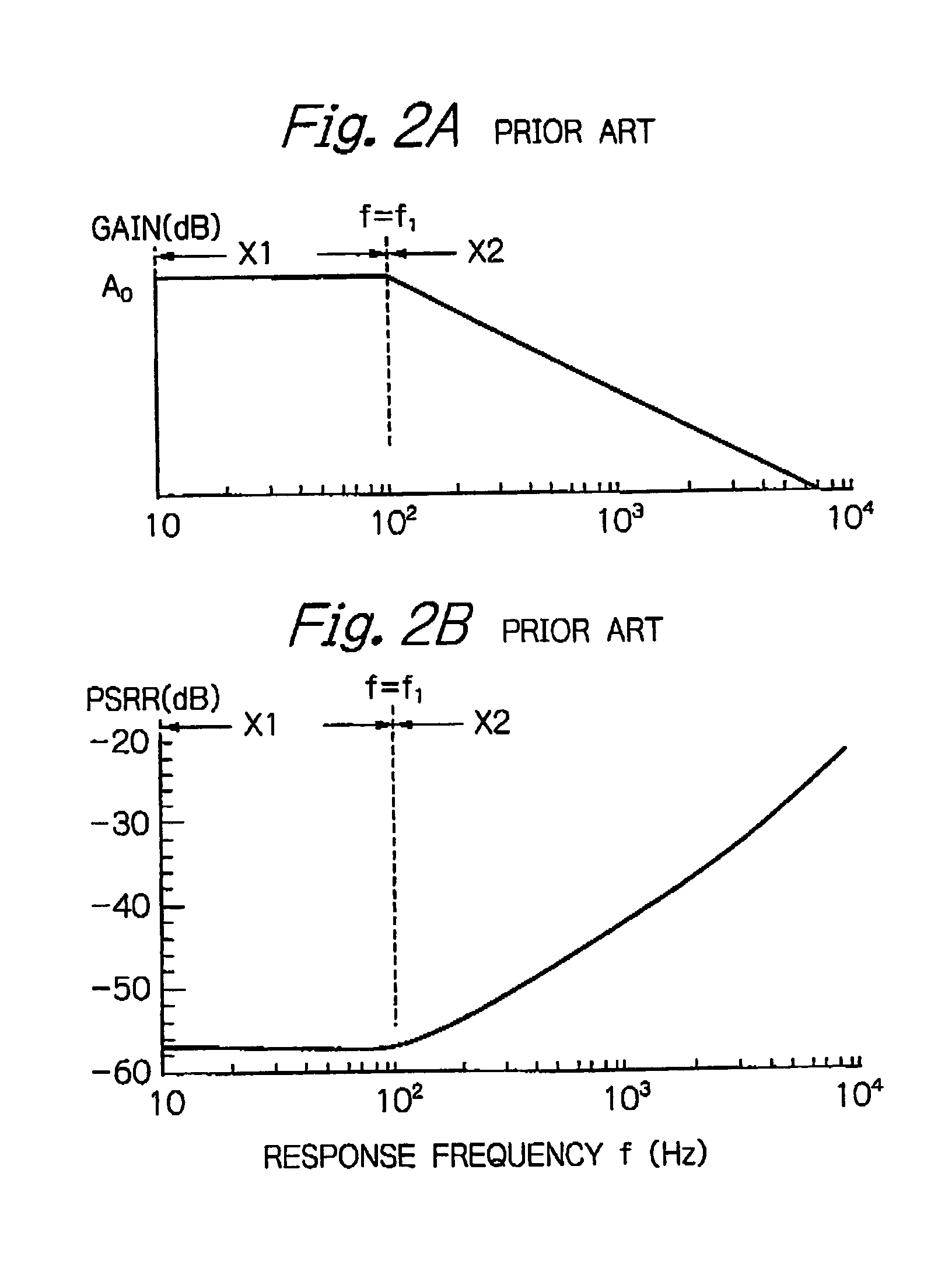
[0039]The gain characteristics of the voltage regulator 10 of FIG. 5 are as shown in FIG. 6A where a response band is limited by the oscillation preventing capacitor 6. Note that since the capacitance of the oscillation preventing capacitor 6 is relatively large, an upper frequency f1 defined by the response band is 80 Hz, for example. Therefore, if a low frequency noise lower than the frequency f1 is applied to the power supply voltage VCC, the negative feedback control using the feedback voltage VFB is carried out to compensate for the low frequency noise, so that the output voltage VOUT is not affected by the low frequency noise.

[0040]On the other hand, the capacitance of the capacitor 7 is determined to pass a high frequency noise higher than the frequency f1 applied to the power supply volta...

second embodiment

[0045]In FIG. 7, which illustrates the voltage regulator according to the present invention, a voltage regulator 20 includes capacitors 21-1, 21-2 and 21-3 associated with switches formed by P-channel MOS transistors 22-1, 22-2 and 22-3, respectively, and a control circuit 23, instead of the capacitor 7 of the voltage regulator 10 of FIG. 5. In this case, the capacitances C1, C2 and C3 of the capacitors 21-1, 21-2 and 21-3 are different from each other, i.e.,

[0046]C123.

[0047]The control circuit 23 is constructed by a voltage detector formed by a P-channel MOS transistor 231 for detecting a source-to-gate voltage of the drive P-channel MOS transistor 5 depending upon the resistance value of the external load 12, a resistor 232 connected to the drain of the P-channel MOS transistor 231, comparators 233 and 234 for comparing a voltage V1 between the P-channel MOS transistor 231 and the resistor 232 with reference voltages VR1 and VR2 (VR1R2), and a gate circuit 235. As a result, when V...

third embodiment

[0048]In FIG. 8, which illustrates the voltage regulator according to the present invention, a voltage regulator 30 includes capacitors 31-1, 31-2 and 31-3, whose capacitances are C0:2C0:4C0, associated with switches (P-channel MOS transistors) 32-1, 32-2 and 32-3, respectively, and a control circuit 33, instead of the capacitor 7 of the voltage regulator 10 of FIG. 5.

[0049]The control circuit 33 is constructed by a voltage detector formed by a P-channel MOS transistor 331 for detecting a source-to-gate voltage of the drive P-channel MOS transistor 5 depending upon the resistance of the load 12, a resistor 332 connected to the drain of the P-channel MOS transistor 331, and an analog / digital (A / D) converter 333 for performing an A / D conversion upon a voltage V1 between the P-channel MOS transistor 331 and the resistor 332 to generate three-bit data (D0, D1, D2). As a result, the switches (P-channel MOS transistors) 32-1, 32-2 and 32-3 are turned ON in accordance with the output signa...


PUM


Abstract

In a voltage regulator, a reference voltage generating circuit generates a reference voltage. A drive transistor is connected between a first power supply terminal and an output terminal and has a control terminal. A voltage divider generates a feedback voltage which is an intermediate voltage between voltages at the output terminal and a first power supply terminal. A differential amplifier generates an error voltage in accordance with the feedback voltage of the voltage divider and the reference voltage, and transmits it to the control terminal of the drive transistor. An oscillation preventing capacitor is connected between the control of the drive transistor and the output terminal. A capacitor is connected between the first power supply terminal and the first input of the differential amplifier.

Description

BACKGROUND OF THE INVENTION[0001]1. Field of the Invention[0002]The present invention relates to a voltage regulator having improved power supply rejection ratio (PSRR) characteristics while maintaining a narrow response band.[0003]2. Description of the Related Art[0004]Voltage regulators have been incorporated in mobile stations such as mobile telephone sets or electronic notebooks which need to be small both in size and power consumption.[0005]In a first prior art voltage regulator (see: FIG. 2 of JP-10-260741-A), a reference voltage generating circuit generates a reference voltage. A drive transistor is connected between a power supply terminal and an output terminal and has a control terminal. A voltage divider generates a feedback voltage which is an intermediate voltage between voltages at the output terminal and the ground terminal. A differential amplifier generates an error voltage in accordance with the feedback voltage of the voltage divider and the reference voltage, and...

Claims


Application Information

Patent Timeline
Patent Type & Authority Patents(United States)
IPC IPC(8): G05F1/565G05F1/56G05F1/40G05F1/575
CPCG05F1/575H04M1/21
Inventor ADACHI, MASAHIRO
Owner RENESAS ELECTRONICS CORP
Why Eureka
Try Eureka