Semiconductor memory device

a memory device and semiconductor technology, applied in the field of semiconductor memory devices, can solve the problems of increasing the manufacturing cost of a semiconductor memory device, the inability to perform high-speed pre-charge, and the inability to read out stored data at high speed, so as to achieve cost advantages

Active Publication Date: 2007-07-31
SOCIONEXT INC
View PDF15 Cites 13 Cited by
  • Summary
  • Abstract
  • Description
  • Claims
  • Application Information

AI Technical Summary

Benefits of technology

[0031]Therefore, an object of the present invention is to provide a semiconductor memory device having a hierarchical bit line structure, which does not require a transistor in which a drain electrode and a source electrode are connected to a main bit line and a sub-bit line, respectively, and can perform a read operation with a low voltage, thereby being advantageous in terms of cost.
[0044]In addition, the semiconductor memory device of the present invention does not include a transistor for causing the main bit line and the sub-bit line to be in conduction with each other. Therefore, a specialized production step or circuit for reducing the substrate bias effect and on-resistance of the transistor is not required, thereby making it possible to reduce the area of the semiconductor memory device and suppress an increase in manufacturing cost.

Problems solved by technology

When a sub-bit line is charged, the influence of the substrate bias effect in the block select transistor reduces the current drive capability of the block select transistor to charge the sub-bit line, so that high-speed precharge cannot be performed.
Therefore, it is not possible to read out stored data with high speed.
Therefore, even when either of the methods is employed, the manufacturing cost of a semiconductor memory device increases.

Method used


Image

  • Semiconductor memory device
  • Semiconductor memory device
  • Semiconductor memory device

Examples


first embodiment

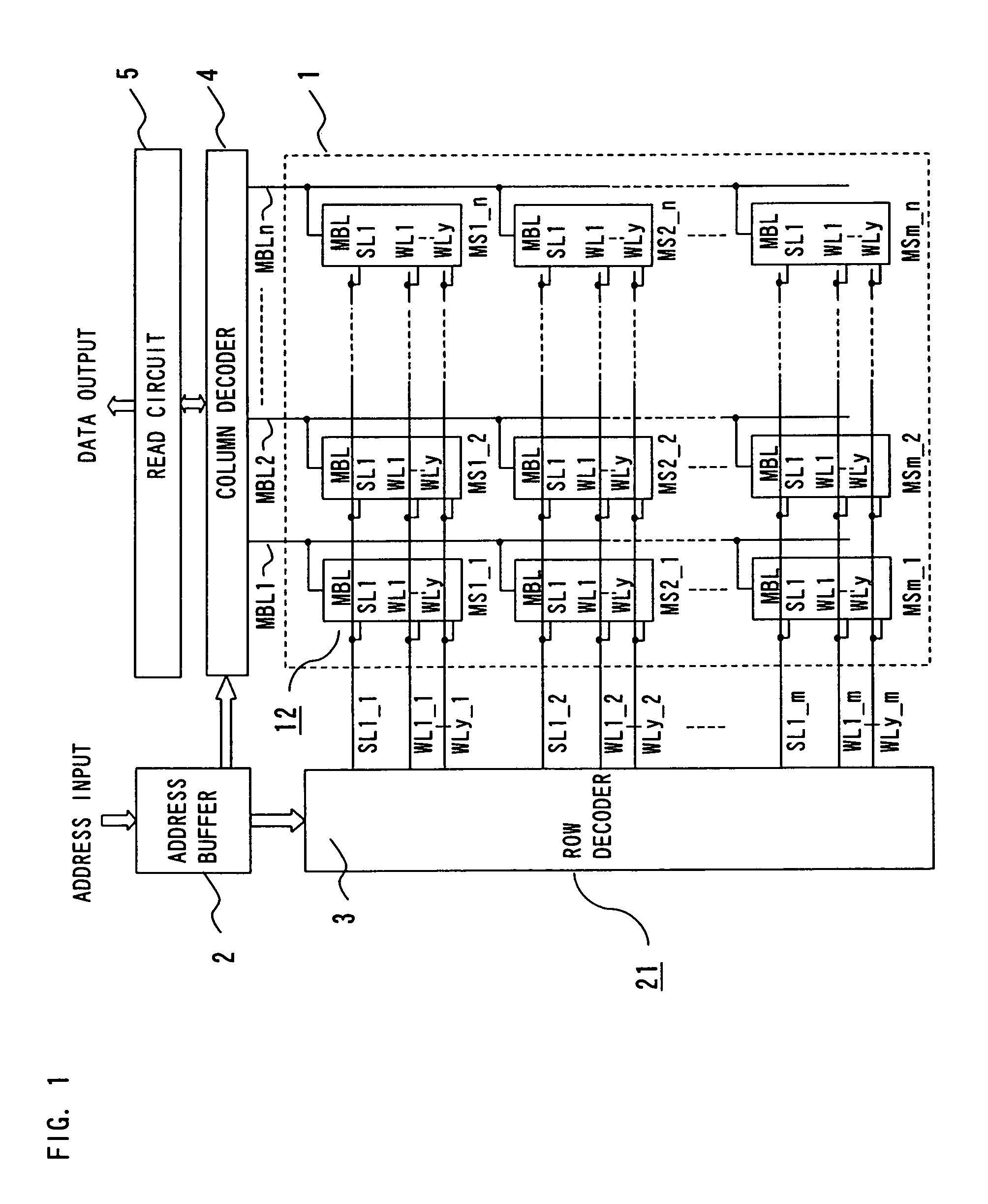
[0061]FIG. 1 is a block diagram illustrating a configuration of a semiconductor memory device according to a first embodiment of the present invention. The semiconductor memory device 21 comprises a memory cell array 1, an address buffer 2, a row decoder 3, a column decoder 4, and a read circuit 5.

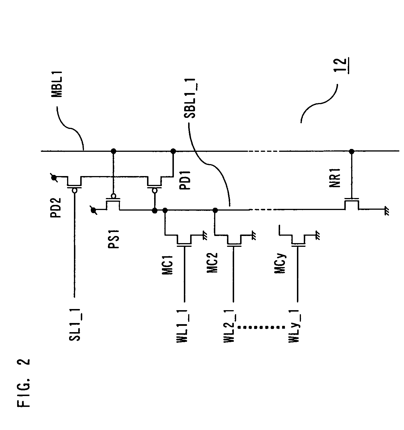
[0062]The memory cell array 1 includes (m×n) subarrays 12 (MS1_1 to MSm_n) arranged in a matrix, m block select lines SL1_1 to SL1_m, (y×m) word lines WL1_1 to WLy_m, and n main bit lines MBL1 to MBLn. The subarrays 12 (MSi_1 to MSi_n) provided on an i-th row are each connected to the block select line SL1_i and the word lines WL1_i to WLy_i. The subarrays 12 (MS1_j to MSm_j) provided on a j-th column are each connected to the main bit line MBLj.

[0063]The address buffer 2 outputs an externally input address to the row decoder 3 and the column decoder 4.

[0064]Based on the address signal output from the address buffer 2, the row decoder 3 selects one block select line (e.g., SL1_i) from the ...

second embodiment

[0093]FIG. 4 is a block diagram illustrating a semiconductor memory device according to a second embodiment of the present invention. The semiconductor memory device 22 comprises a memory cell array 6, an address buffer 2, a row decoder 7, a column decoder 4, and a read circuit 5. Note that the address buffer 2, the column decoder 4, and the read circuit 5 are configured in a manner similar to that of the first embodiment and will not be hereinafter described.

[0094]The memory cell array 6 includes (m×n) subarrays 13 (MS1_1 to MSm_n) arranged in a matrix, m first the block select lines SL1_1 to SL1_m, m second block select lines SL2_1 to SL2_m, (y×m) word lines WL1_1 to WLy_m, and n main bit lines MBL1 to MBLn. The subarrays 13 (MSi_1 to MSi_n) provided on an i-th row are each connected to the first block select line SL1_i, the second block select line SL2_i, and the word lines WL1_i to WLy_i. The subarrays 13 (MS1_j to MSm_j) provided on a j-th column are each connected to the main ...

third embodiment

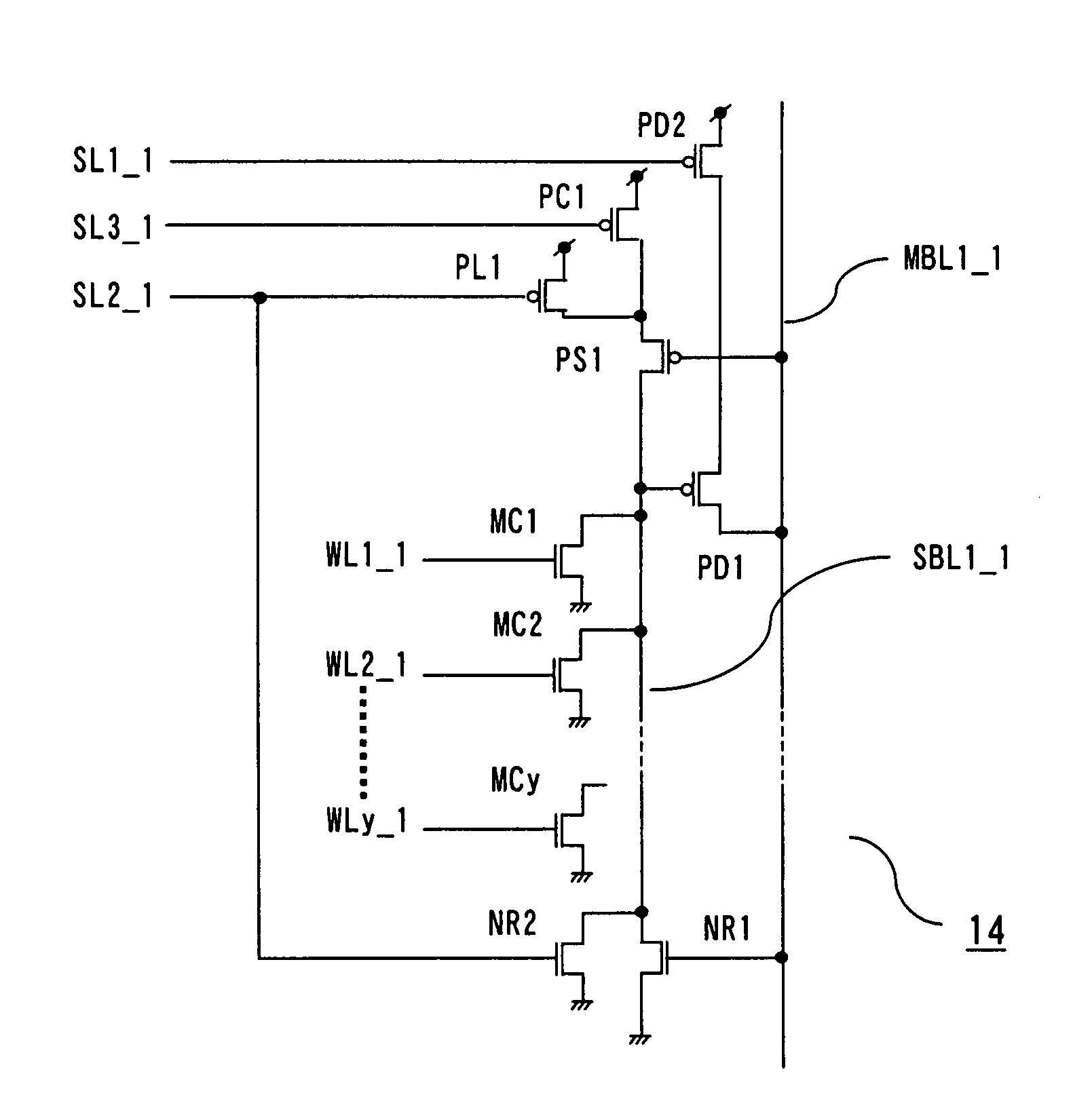
[0121]FIG. 7 is a block diagram illustrating a configuration of a semiconductor memory device according to a third embodiment of the present invention. The semiconductor memory device 23 comprises a memory cell array 8, an address buffer 2, a row decoder 9, a column decoder 4, and a read circuit 5. Note that the address buffer 2, the column decoder 4, and the read circuit 5 are configured in a manner similar to that of the first embodiment, and will not be hereinafter described.

[0122]The memory cell array 8 includes (m×n) subarrays 14 (MS1_1 to MSm_n) arranged in a matrix, m first block select lines SL1_1 to SL1_m, m second block select lines SL2_1 to SL2_m (not shown), m third block select lines SL3_1 to SL3_m, (y×m) word lines WL1_1 to WLy_m, and n main bit lines MBL1 to MBLn. The subarrays 14 (MSi_1 to MSi_n) provided on an i-th row are each connected to the first block select line SL1_i, the second block select line SL2_i, the third block select line SL3_i, and the word lines WL...


PUM


Abstract

A semiconductor memory device is provided which has a hierarchical bit line structure and can perform a high-speed read operation even with a low voltage. A subarray 12 includes a first MOS transistor PD1 for charging a main bit line MBL1 and a second MOS transistor PS1 for charging a sub-bit line SBL1—1. The source electrode of the second MOS transistor PS1 is connected to a power source voltage, and the source electrode of the first MOS transistor PD1 is connected via a fourth MOS transistor PD2 to the power source voltage. Since there is not a resistance between the main bit line MBL1 and the sub-bit line SBL1—1, which is present if a transistor is used to achieve conduction therebetween, discharging of the main bit line and charging of the sub-bit line can be performed with high speed.

Description

BACKGROUND OF THE INVENTION[0001]1. Field of the Invention[0002]The present invention relates to a semiconductor memory device, and more particularly, to a semiconductor memory device having a hierarchical bit line structure.[0003]2. Description of the Background Art[0004]In conventional semiconductor memory devices, bit lines are hierarchically arranged in order to prevent the level of the bit line from being reduced due to a cut-off leakage current. For example, Japanese Patent Laid-Open Publication No. 6-176592 (p. 2, FIG. 2) discloses a mask ROM having a contact, as an example of such a semiconductor memory device having a hierarchical bit line structure.[0005]FIG. 13 is a block diagram illustrating a configuration of a conventional mask ROM. The mask ROM 50 comprises a memory cell array 51, an address buffer 52, a row decoder 53, a column decoder 54, and a read circuit 55.[0006]The memory cell array 51 comprises (m×n) subarrays 57 (MS1_1 to MSm_n) arranged in a matrix, m block ...

Claims


Application Information

Patent Timeline
Patent Type & Authority Patents(United States)
IPC IPC(8): G11C8/00
CPCG11C7/12G11C7/18G11C17/12
Inventor NAKAYA, SHUJIABE, WATARUHAYASHI, MITSUAKI
Owner SOCIONEXT INC
Why Eureka
Try Eureka