
LED array package with internal feedback and control

a technology of led arrays and feedback circuits, which is applied in the direction of lighting and heating apparatuses, semiconductor devices for light sources, solid-state devices, etc., can solve the problems of circuitry, cost and complexity of additional detectors, and significant heat generated by dense concentrations of leds

Active Publication Date: 2007-08-07
LIGHTING SCI GROUP
View PDF52 Cites 294 Cited by
  • Summary
  • Abstract
  • Description
  • Claims
  • Application Information

AI Technical Summary

Benefits of technology

"The invention is a packaged LED array that can operate at high temperatures. It includes a metal base with a thermal connection pad and layers of ceramic. The LED dice are thermally coupled to the metal base and have electrodes. A driver circuit is mounted within the package and connected to the LED die electrodes to control the current. The LED dice can also be switched to act as a photodetector to measure the light output of the LED array and use that information to control the light output."

Problems solved by technology

One problem with LED arrays is the significant heat generated by dense concentrations of LEDs.
Another problem associated with LED array performance, illumination efficiency, is the subject of a related application entitled “Efficient LED Array”, U.S. patent application Ser. No. 10 / 822,191, filed Apr. 9, 2004.
The problem is the cost and complexity of the additional detector and the mechanical construction required to mount it in or near the array.
Such circuitry is needed but has been difficult to package on the same substrate as the LEDs.
This is problematic for applications that must fit into small spaces.
LED arrays using external PCB mounted electronics are also costly.
Previous attempts to incorporate driver circuitry into LED array packages have largely been unsuccessful because of the mechanical stresses caused by differences in the thermal coefficients of expansion between semiconductor die and prior art LED packaging methods and materials.

Method used


Image

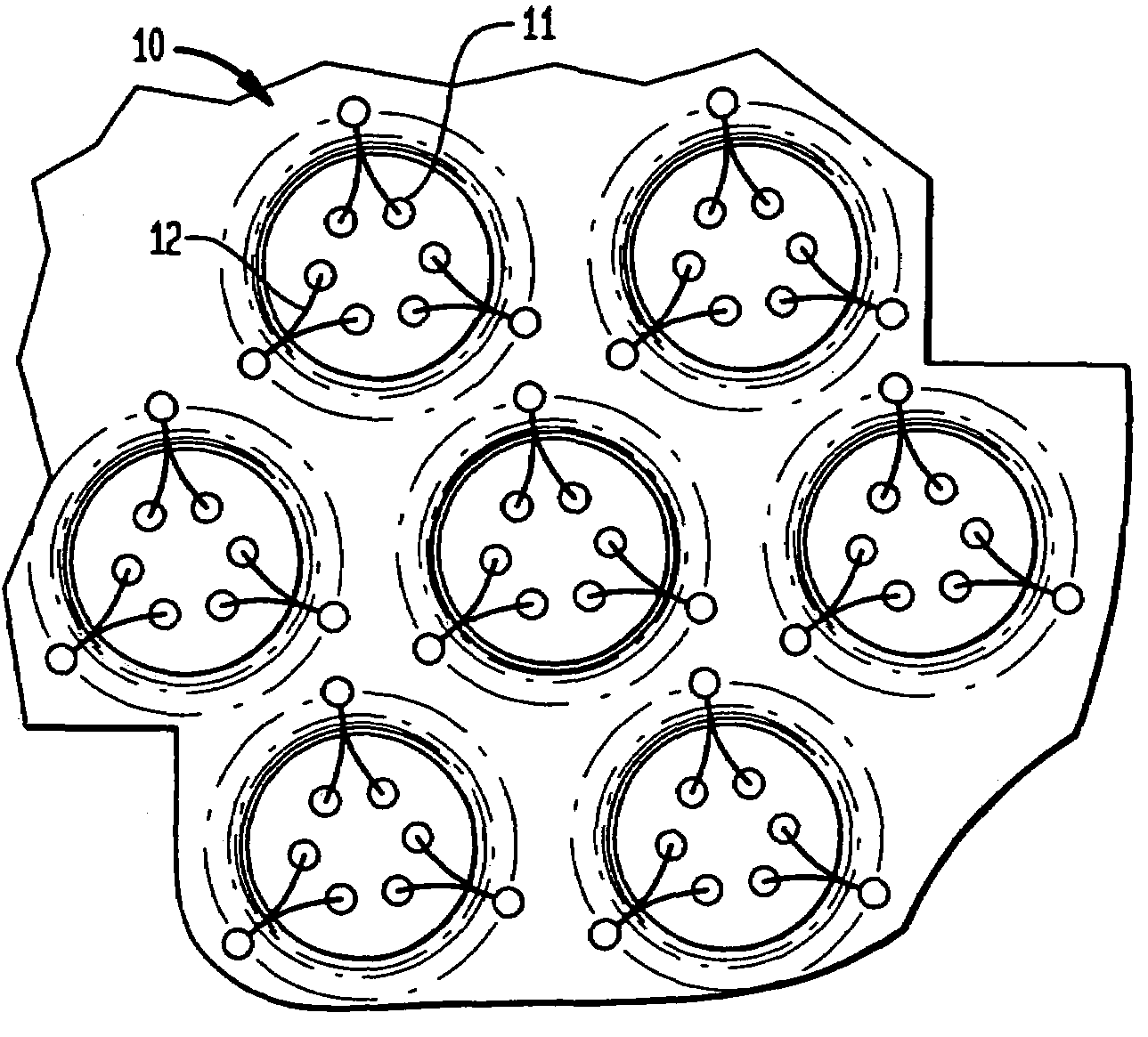
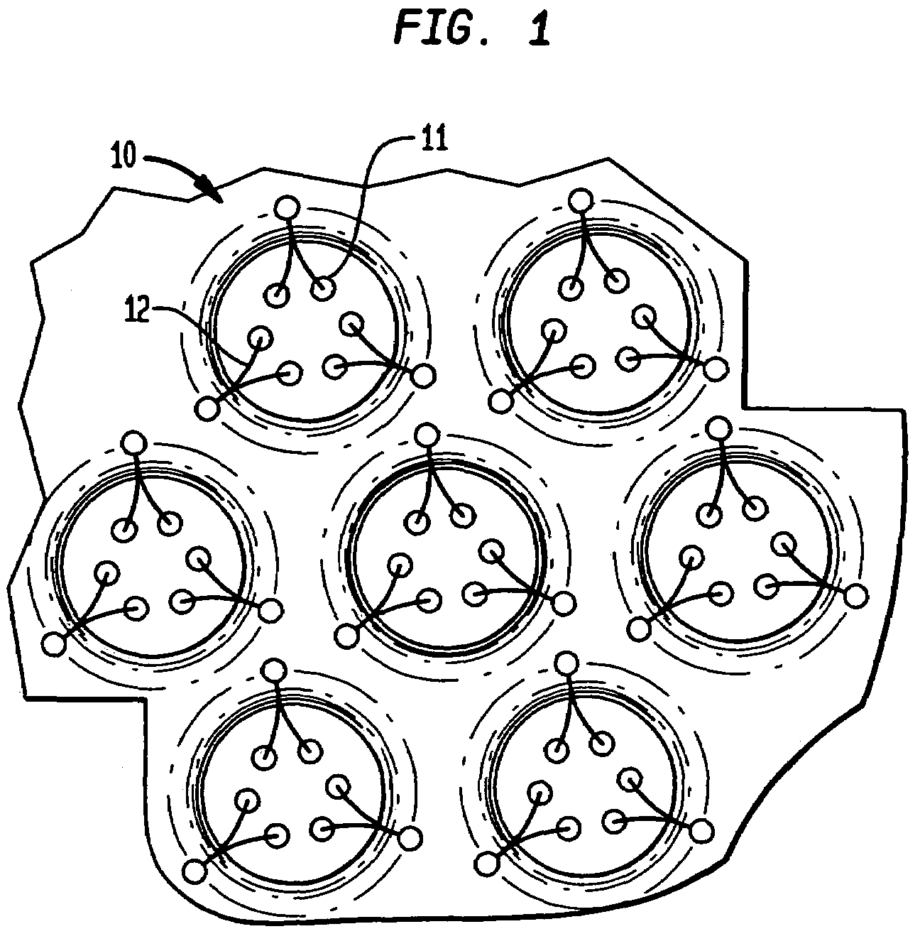
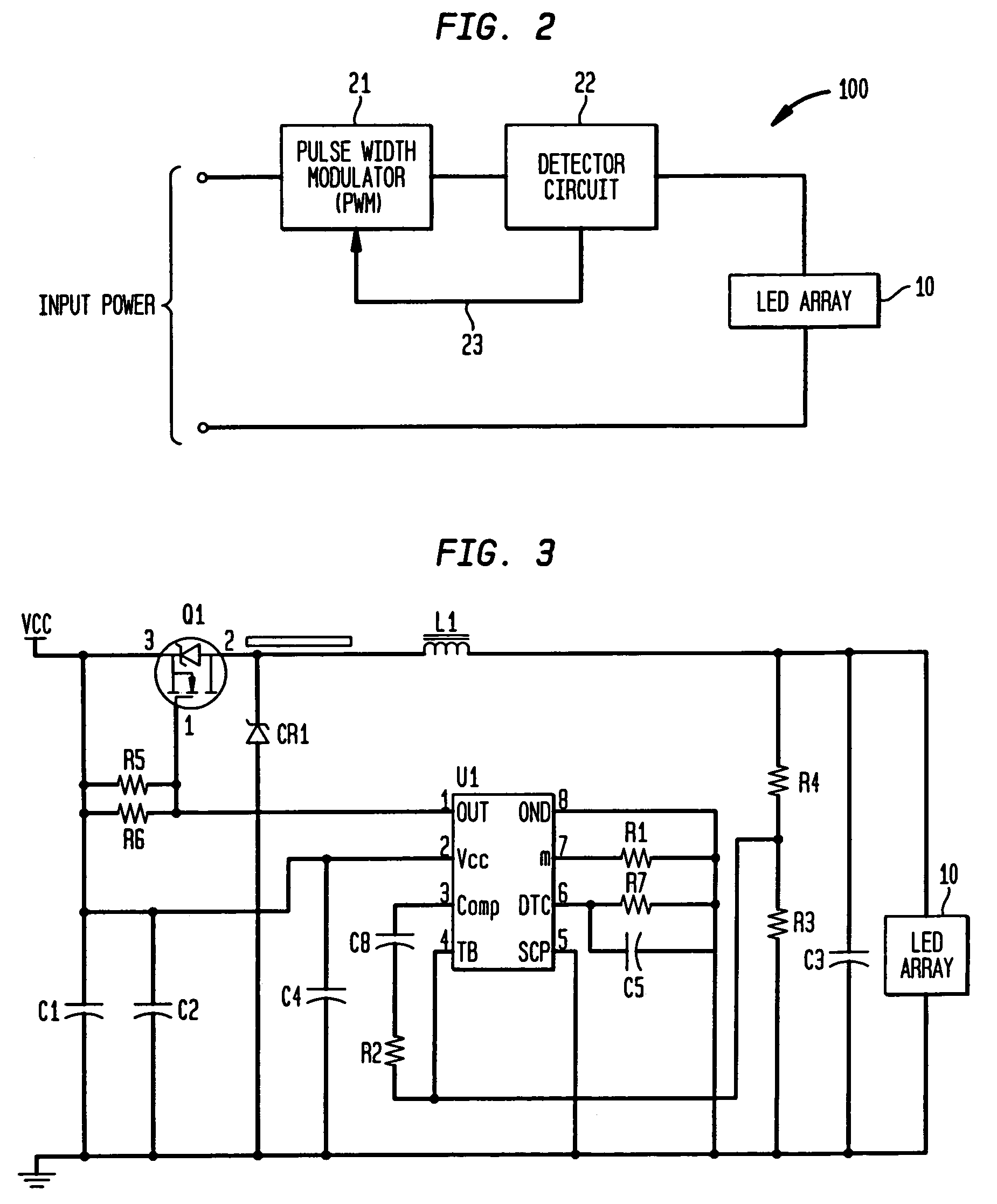
  • LED array package with internal feedback and control
  • LED array package with internal feedback and control
  • LED array package with internal feedback and control

Examples


example

[0039]The following is an example of a device comprising co-packaging light emitting diode arrays wherein one or more of the LEDs are used as a photodetector to detect the light output of the LED array. The device is constructed beginning with a suitable metal laminate base. Preferably, a 13% copper, 74% molybdenum, 13% copper (CMC) metal laminate is used. More preferably, the CMC metal laminate produced by H. C. Starck Corporation, Newton, Mass., can be used in accordance with the invention.

[0040]Thick film gold bonding pads, corresponding to the location of each die, can be fired on the metal base to include LED die and any die used for control and feedback purposes. The pads can be connected electrically and thermally to the CMC base. Layers of CMC-compatible ceramic tape can be used to form the die cavities, to make the electrical connections, and to form the array housing. The ceramic tape is composed of glasses and resins which are readily commercially available, including, bu...


PUM


Abstract

A packaged LED array for high temperature operation comprises a metal base, the metal base including an underlying thermal connection pad. One or more layers of ceramic overly the metal base. The array includes a plurality of LED dice, each LED die having electrodes. And, the LED thermally coupled to the metal base. A driver circuit is electrically connected to the LED die electrodes and controls the LED array current. An LED driver is mounted within the LED array package, and thermally coupled to the metal base. In a second embodiment, one or more of the LED dice can be switched from the driver to a measurement circuit and used as a photodetector to measure the light output of the LED array. The measured photodetector signal can further be used as a feedback signal to control the LED array light output.

Description

FIELD OF THE INVENTION[0001]This invention relates to an apparatus for co-packaging light emitting diode (LED) arrays with electronic driver and feedback circuitry wherein the electronic driver and control circuitry are incorporated within the LED array package. The invention also relates to, a method and apparatus for monitoring and controlling the LED array light output using one or more dice of the LED array as a photodetector.BACKGROUND OF THE INVENTION[0002]Light emitting diodes (LEDs) are useful in a wide variety of applications. An LED array is an array of LED die mounted on a common substrate. LED arrays are used as light sources in an increasing variety of applications including communications and instrumentation; commercial and household room lighting; and automotive and visual displays. LED Arrays are devices comprising a plurality of LEDs on the same substrate. LED arrays can be made by a variety of techniques.[0003]One problem with LED arrays is the significant heat gen...

Claims


Application Information

Patent Timeline
Patent Type & Authority Patents(United States)
IPC IPC(8): H01L29/22F21K99/00H01L33/00H01L33/08H01L33/48H01L33/64
CPCF21K9/00H01L2224/48091H01L2224/48137H01L2224/73265H01L2924/10155F21V23/005F21V23/0457H05B45/22H05B45/3725H01L2924/00014
Inventor MAZZOCHETTE, JOSEPHBLONDER, GREG E.
Owner LIGHTING SCI GROUP
Learn More