Method and arrangement for performing atomic updates using a logical flash memory device
- Summary
- Abstract
- Description
- Claims
- Application Information
AI Technical Summary
Benefits of technology
Problems solved by technology
Method used
Image
Examples
Embodiment Construction
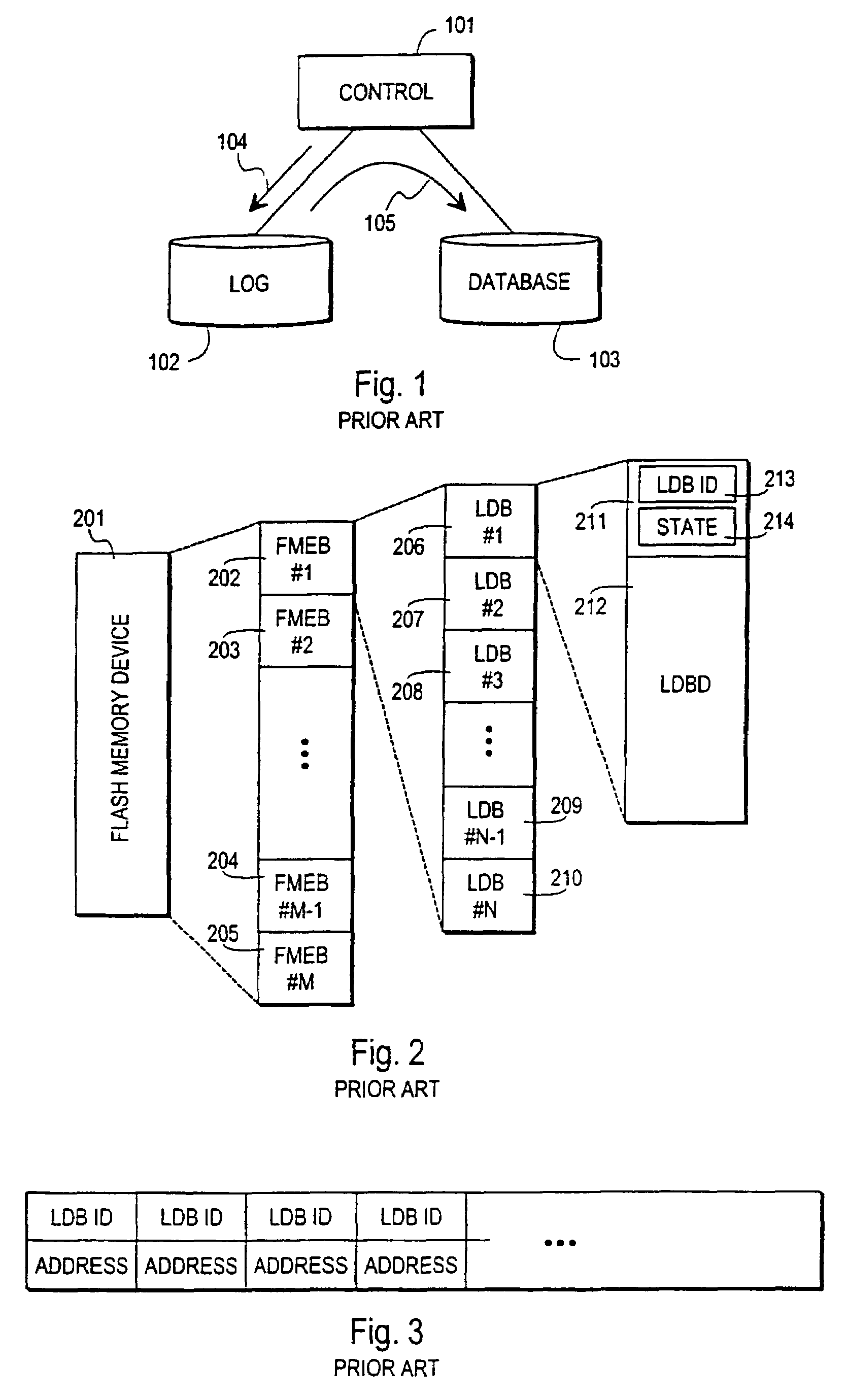
[0044]FIG. 1 has been treated above in the description of prior art, so the following description of the invention with its advantageous embodiments will focus on FIGS. 2 to 11.
[0045]To provide full understanding of the invention we will first briefly describe some known features of flash memories and other devices that have logically a similar structure and operation. Flash memory data cannot generally be updated to the same physical memory position without first erasing a complete logical block of memory. After a block level erasure all bits within the erased block have a common first constant value, usually 1. Each bit within the block can then be separately written once by changing its value to a second constant value, usually 0. Thereafter the only way to change the value of the bit is to erase the whole block again.
[0046]FIG. 2 illustrates schematically a flash memory device 201 which is divided into Flash Memory Erase Blocks or FMEBs. There are in general a large positive int...
PUM
 Abstract
Description
Claims
Application Information


