Supercharge Your Innovation With Domain-Expert AI Agents!

Manufacture of a semiconductor integrated circuit device including a pluarality of a columnar laminates having different spacing in different directions

a technology of integrated circuit devices and columns, which is applied in the direction of transistors, spraying devices, instruments, etc., can solve the problems of difficult filling of insulating films between, and achieve the effects of improving filling properties, miniaturizing devices, and improving the properties of semiconductor integrated circuit devices

Inactive Publication Date: 2007-08-21
RENESAS ELECTRONICS CORP
View PDF14 Cites 6 Cited by
  • Summary
  • Abstract
  • Description
  • Claims
  • Application Information

AI Technical Summary

Benefits of technology

This approach improves the filling properties between vertical MISFETs, enabling miniaturization and enhancing the overall performance of semiconductor integrated circuit devices by ensuring precise and effective insulation.

Problems solved by technology

It has been revealed that when vertical type MISFETs are employed, it becomes difficult to fill an insulating film between them.

Method used


Image

  • Manufacture of a semiconductor integrated circuit device including a pluarality of a columnar laminates having different spacing in different directions
  • Manufacture of a semiconductor integrated circuit device including a pluarality of a columnar laminates having different spacing in different directions
  • Manufacture of a semiconductor integrated circuit device including a pluarality of a columnar laminates having different spacing in different directions

Examples


Embodiment Construction

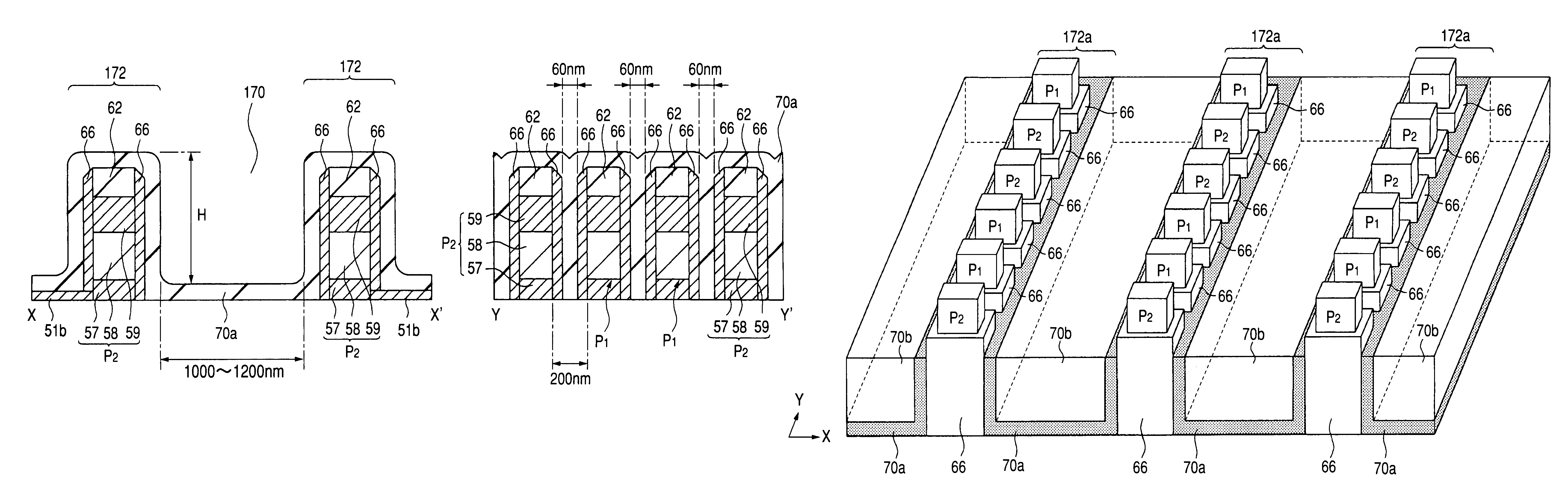
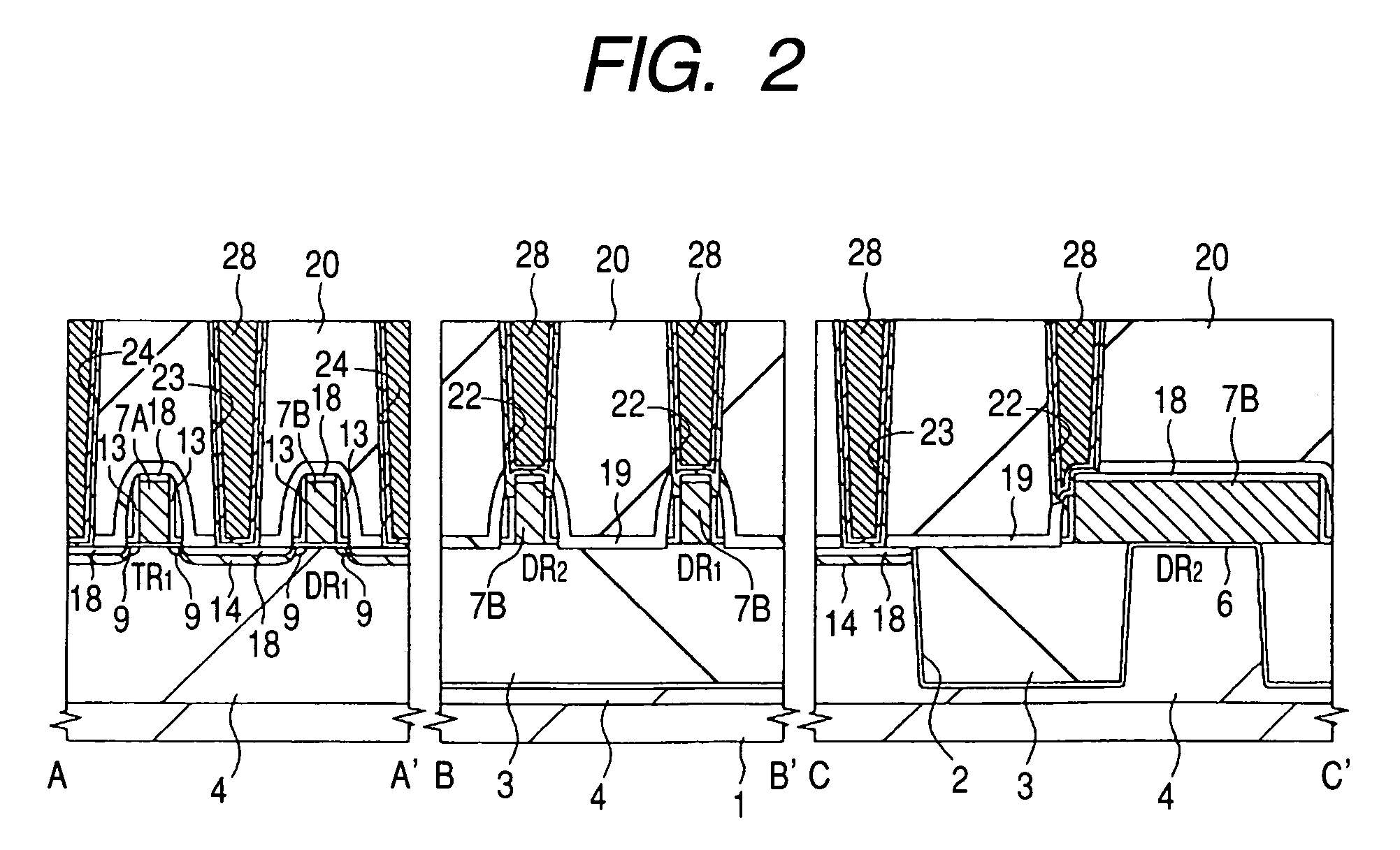
[0065]The embodiments of the present invention will hereinafter be described specifically with reference to the accompanying drawings. In all of the drawings, members having a like function will be identified by like reference numerals and overlapping descriptions thereof will be omitted. To facilitate an understanding of the description, some parts (for example, an insulating film) will be described with reference to an ordinal number “first”, “second” or the like, but this does not always correspond to the terms “first”, “second” or the like as used in the appended claims.

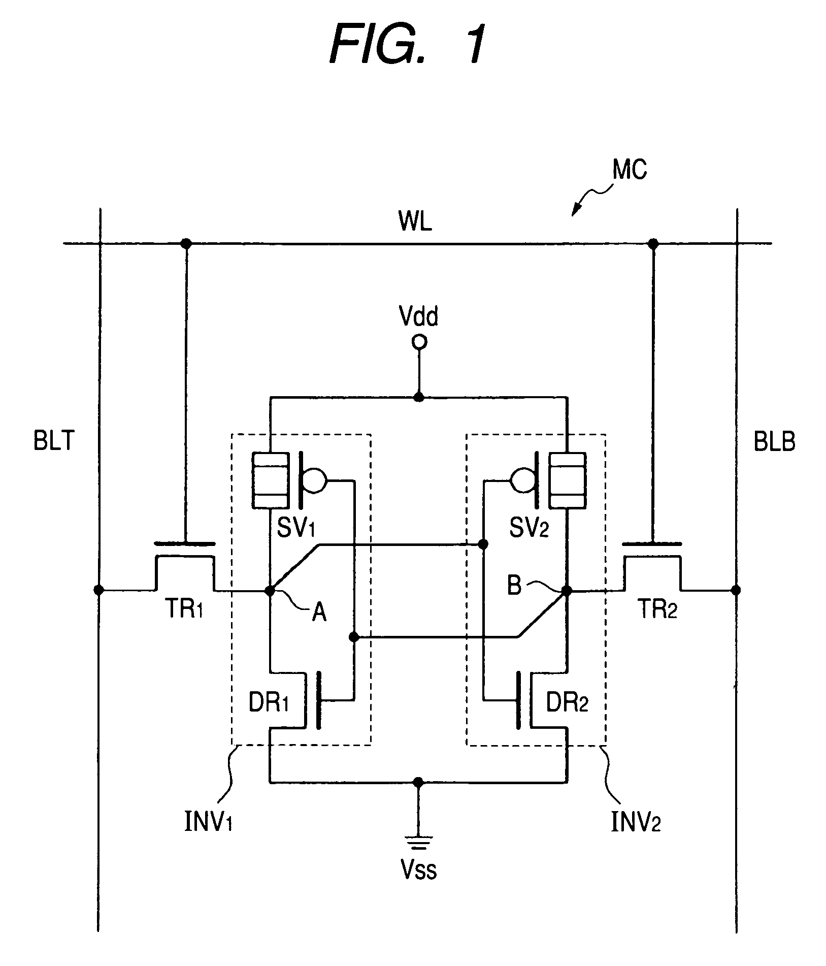
[0066]FIG. 1 is an equivalent circuit diagram of a memory cell of a SRAM according to an embodiment of the present invention. As illustrated in FIG. 1, memory cells (MC) of the SRAM are each constituted of two horizontal transfer MISFETs (TR1 and TR2, each of which will hereinafter simply be called a “transfer MISFET”), two horizontal drive MISFETs (DR1 and DR2, each of which will hereinafter simply be called a “...


PUM


Abstract

For improving the filling properties between vertical MISFETs constituting a SRAM memory cell, the vertical MISFETs are formed over horizontal drive MISFETs and transfer MISFETs, and they are disposed with a narrow pitch in the Y direction and a wide pitch in the X direction. After a first insulating film (O3-TEOS) having good coverage is disposed over columnar laminates having a lower semiconductor layer, an intermediate semiconductor layer, an upper semiconductor layer and a silicon nitride film and a gate electrode formed over the side walls of the laminates via a gate insulating film to completely fill a narrow pitch space, a second insulating film (HDP silicon oxide film) is deposited over the first insulating film, resulting in an improvement in the filling properties, even in a narrow pitch portion, between vertical MISFETs having a high aspect ratio.

Description

TECHNICAL FIELD[0001]The present invention relates to a semiconductor integrated circuit device and to a technique for use in the manufacture thereof; and, more particularly, the invention relates to a technique that is effective when applied to a semiconductor integrated circuit device having a vertical MISFET.BACKGROUND OF THE INVENTION[0002]Semiconductor integrated circuit devices have many layer-stack structures, each having a conductive film and an insulating film. The insulating film tends to be formed in order to insulate between conductive films. For example, plural interconnect layers are separated by an insulating film. An element formation region of a semiconductor substrate is also separated by an insulating film that has been filled in a groove.[0003]The space between interconnects or a groove space, however, tends to be narrower with a recent tendency toward high integration and miniaturization of the device. In some parts, the ratio of the width to the height of a spa...

Claims


Application Information

Patent Timeline
Patent Type & Authority Patents(United States)
IPC IPC(8): H01L21/8238H01L23/522H10B12/00G11C11/412H01L21/316H01L21/768H01L21/8234H01L27/088H01L29/76H10B10/00
CPCG11C11/412H01L29/7827H01L27/1104H01L29/66666H01L27/11H01L27/0207H10B10/00H10B10/12B05B7/04
Inventor MURATA, TATSUNORINAKAMURA, TAKAHIROSUZUKI, YASUMICHI
Owner RENESAS ELECTRONICS CORP
Features
  • R&D
  • Intellectual Property
  • Life Sciences
  • Materials
  • Tech Scout
  • Unparalleled Data Quality
  • Higher Quality Content
  • 60% Fewer Hallucinations
Learn More