Visual or multimedia interface bus switch with level-shifted ground and input protection against non-compliant transmission-minimized differential signaling (TMDS) transmitter

a level-shifted ground and bus switch technology, applied in logic circuits, pulse automatic control, pulse techniques, etc., can solve the problems that the bus switch chip b>10/b> designed for 3.3-volt power supplies may have too much capacitance, and the use of a 2.0-volt vcc with the bus switch chip b>10/b> does not appear to be useful for switching tmds signals that operate at 2.7-3.3 volts

Inactive Publication Date: 2007-08-21
DIODES INC
View PDF17 Cites 29 Cited by
  • Summary
  • Abstract
  • Description
  • Claims
  • Application Information

AI Technical Summary

Problems solved by technology

Thus simply using a 2.0-volt Vcc with bus switch chip 10 does not appear to be useful for switching TMDS signals that operates at 2.7-3.3 volts.
However, bus switch chip 10 designed for 3.3-volt power supplies may have too much capacitance due...

Method used


Image

  • Visual or multimedia interface bus switch with level-shifted ground and input protection against non-compliant transmission-minimized differential signaling (TMDS) transmitter
  • Visual or multimedia interface bus switch with level-shifted ground and input protection against non-compliant transmission-minimized differential signaling (TMDS) transmitter
  • Visual or multimedia interface bus switch with level-shifted ground and input protection against non-compliant transmission-minimized differential signaling (TMDS) transmitter

Examples


Embodiment Construction

[0023]The present invention relates to an improvement in bus switches. The following description is presented to enable one of ordinary skill in the art to make and use the invention as provided in the context of a particular application and its requirements. Various modifications to the preferred embodiment will be apparent to those with skill in the art, and the general principles defined herein may be applied to other embodiments. Therefore, the present invention is not intended to be limited to the particular embodiments shown and described, but is to be accorded the widest scope consistent with the principles and novel features herein disclosed.

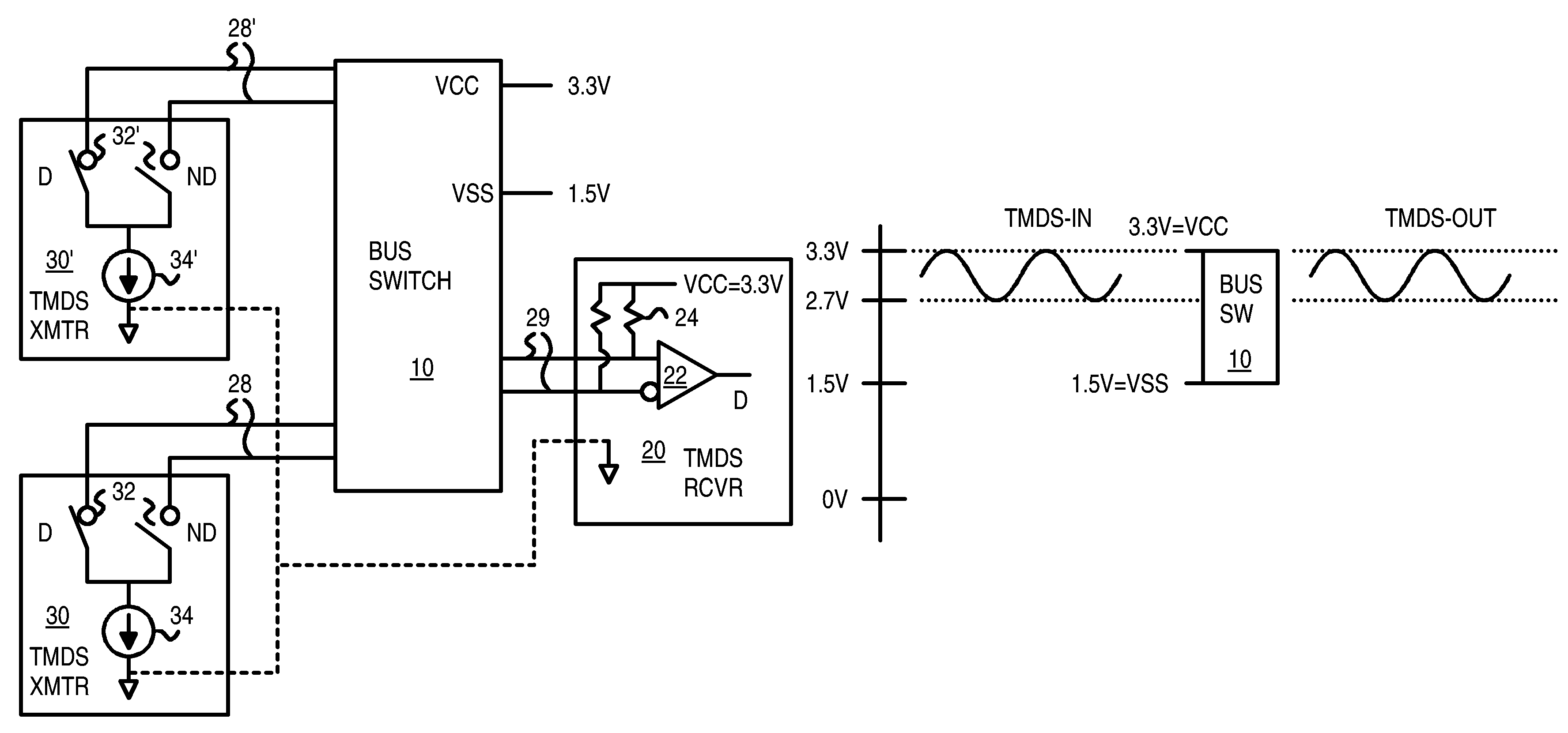
[0024]The inventors have realized that a bus switch chip designed for a reduced 2.0-volt power supply may be used for switching elevated TMDS voltage swings by shifting upward both the ground and power supply voltage applied to the bus switch chip. Rather than apply a 2.0 or 1.8 volt power supply and a 0-volt ground to bus switch chip 10...


PUM


Abstract

A bus switch chip is limited to operating with a power-supply voltage of 1.8 volts relative to a 0-volt ground. Differential bus signals switched through the bus switch chip swing from 2.7 to 3.3 volts, well above the chip's specified power-supply voltage. The bus switch chip is level-shifted by applying a 1.5-volt signal as the chip's ground, and a 3.3-volt signal as its power supply, so the chip's net power supply is within the specification at 1.8 volts. High-Definition Multimedia Interface (HDMI) and Digital Visual Interface (DVI) require that the differential signals are never driven to ground. However, some non-compliant video transmitters drive differential signals to ground when disabled. External pullup resistors or internal pullup transistors in the bus switch chip are added to the bus signals from non-compliant transmitters to pull disabled signals above the 1.5-volt chip ground to prevent damage from signals below the chip's 1.5-volt ground.

Description

FIELD OF THE INVENTION[0001]This invention relates to bus switches, and more particularly to level-shift applications for bus switches.BACKGROUND OF THE INVENTION[0002]Bus switches are useful for a variety of applications such as telecommunications, personal computer (PC), networking, and graphics. The basic, simple structure of a transistor bus switch is ideal for higher speed applications. Bus switches may have many transistors in parallel that are packaged together in a single integrated circuit (IC) chip package, allowing for parallel signals on a bus to be switched together.[0003]FIG. 1 shows a prior-art bus switch. Bus switch chip 10 multiplexes an A bus and a B bus, that are connected on the left, to a C bus connected on the right. A control or select signal CSEL is input to bus switch chip 10 and is buffered by non-inverting buffer 16 to generate ASEL and inverter 18 to generate BSEL. When ASEL is high, BSEL is low, and bus-switch transistors 12 are turned on and bus-switch ...

Claims


Application Information

Patent Timeline
IPC IPC(8): H03K19/0175H03K19/096
CPCH03K19/0185H03K19/096
Inventor HUI, CHI-HUNGLI, XIANXIN
Owner DIODES INC
Why Eureka
Try Eureka