Operation of multiple select gate architecture

a technology of select gate and operation gate, which is applied in the direction of semiconductor devices, digital storage, instruments, etc., can solve the problems of increasing leakage current and decreasing the size of the device, and achieve the same level of protection, reduce the footprint of the nand string, and reduce the size of the memory devi

Active Publication Date: 2007-08-21
MICRON TECH INC
View PDF10 Cites 33 Cited by
  • Summary
  • Abstract
  • Description
  • Claims
  • Application Information

AI Technical Summary

Benefits of technology

[0013]Non-volatile memory devices are described utilizing a NAND architecture including multiple series-coupled select gates on the drain and / or source ends of the NAND strings. By utilizing multiple series-coupled select gates, each gate can be made using smaller features sizes while achieving the same level of protection against GIDL and other forms of current leakage. By reducing the feature size of the select gates, the footprint of the NAND strings can be reduced, thereby facilitating smaller memory device sizing. While the invention is described with reference to NAND architecture memory devices, the concepts of the invention are applicable to other array architectures utilizing select gates for access to strings of memory cells between a bit line and a source, e.g., AND architecture memory devices or the like.

Problems solved by technology

Unfortunately, there can be resulting problems with decreasing device sizes.
For example, as the channel length and gate oxide thickness are reduced in a field-effect transistor, leakage current generally increases.
GIDL can cause a problem referred to as program disturb during a programming operation of a flash memory array.

Method used


Image

  • Operation of multiple select gate architecture
  • Operation of multiple select gate architecture
  • Operation of multiple select gate architecture

Examples


Embodiment Construction

[0019]In the following detailed description of the present embodiments, reference is made to the accompanying drawings that form a part hereof, and in which is shown by way of illustration specific embodiments in which the inventions may be practiced. These embodiments are described in sufficient detail to enable those skilled in the art to practice the invention, and it is to be understood that other embodiments may be utilized and that process, electrical or mechanical changes may be made without departing from the scope of the present invention. The following detailed description is, therefore, not to be taken in a limiting sense, and the scope of the present invention is defined only by the appended claims and equivalents thereof.

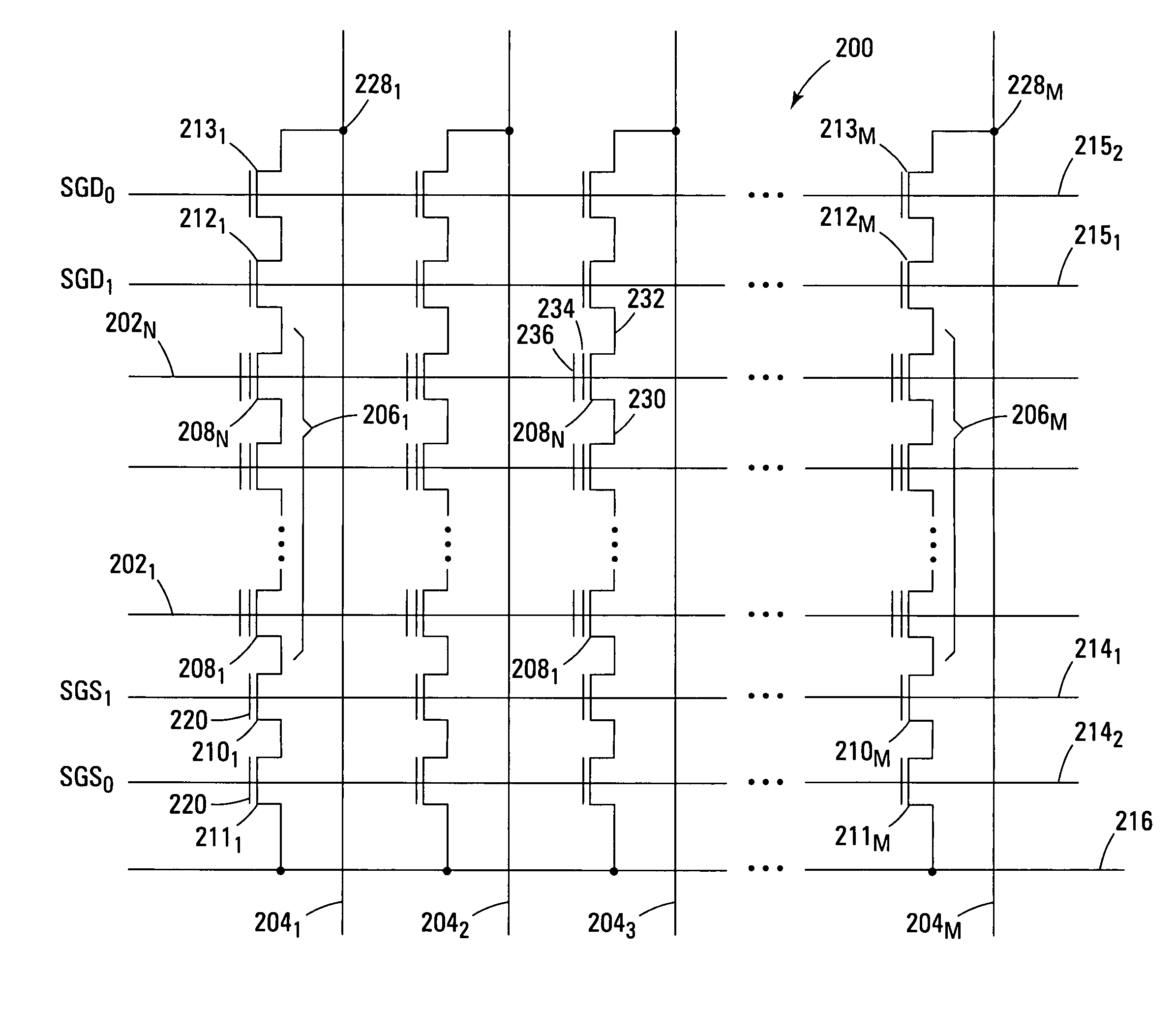
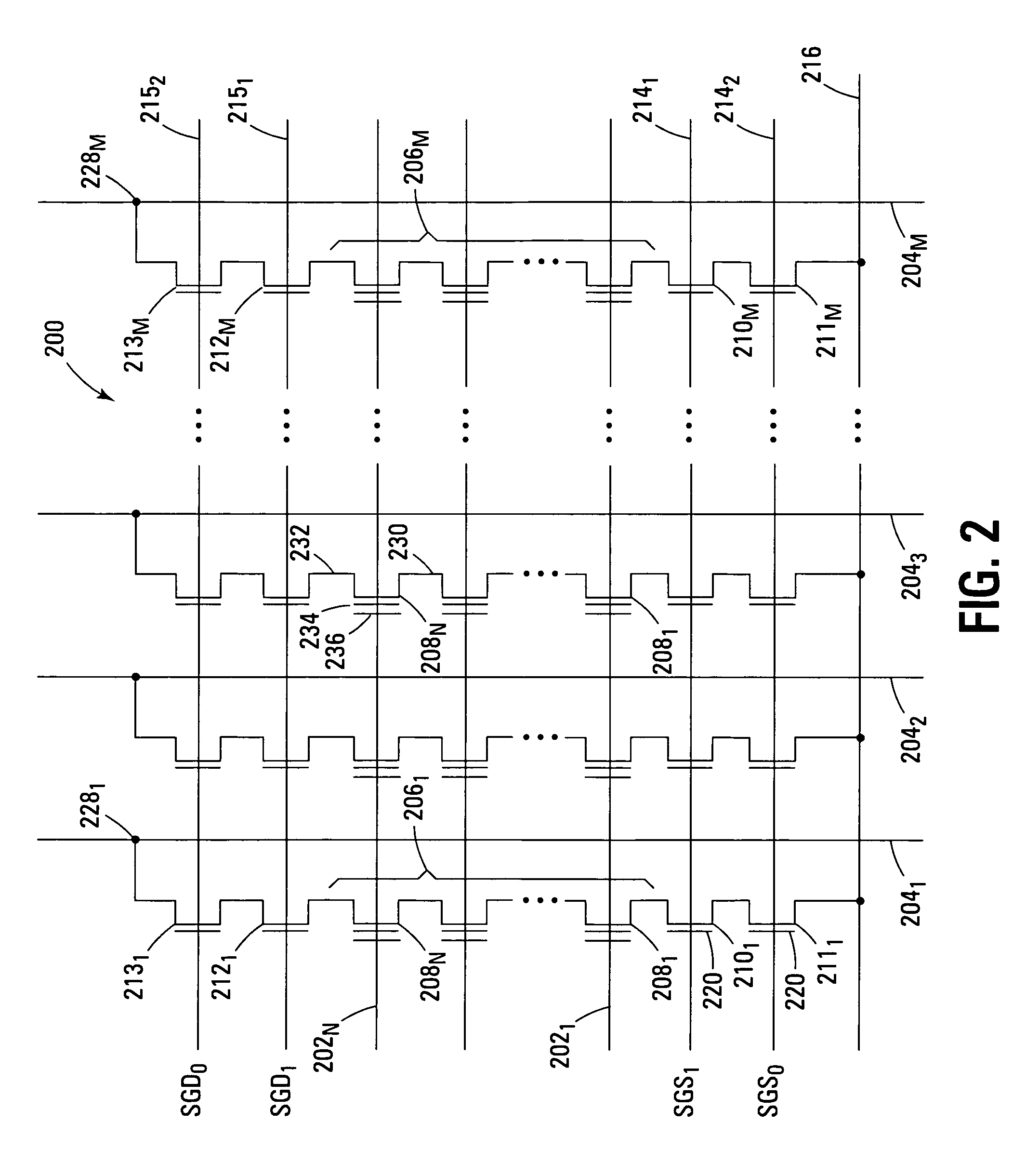
[0020]FIG. 2 is a schematic of a portion of a NAND memory array 200 in accordance with an embodiment of the invention. As shown in FIG. 2, the memory array 200 includes word lines 2021 to 202N and intersecting bit lines 2041 to 204M. For ease of address...


PUM


Abstract

Methods of operating non-volatile memory devices including multiple series-coupled select gates on the drain and / or source ends of strings of non-volatile memory cells facilitate mitigation of gate-induced drain leakage and program disturb.

Description

RELATED APPLICATION[0001]This application is related to U.S. patent application Ser. No. 11 / 216,755 filed Aug. 31, 2005 and commonly assigned.TECHNICAL FIELD OF THE INVENTION[0002]The present invention relates generally to semiconductor memory devices, and in particular, the present invention relates to operation of memory devices having multiple select gates for drain side and / or source side of, for example, NAND strings.BACKGROUND OF THE INVENTION[0003]Memory devices are typically provided as internal, semiconductor, integrated circuits in computers or other electronic devices. There are many different types of memory including random-access memory (RAM), read only memory (ROM), dynamic random access memory (DRAM), synchronous dynamic random access memory (SDRAM), and flash memory.[0004]Flash memory devices have developed into a popular source of non-volatile memory for a wide range of electronic applications. Flash memory devices typically use a one-transistor memory cell that al...

Claims


Application Information

Patent Timeline
Patent Type & Authority Patents(United States)
IPC IPC(8): G11C16/04
CPCG11C16/0483G11C16/12G11C16/3427H01L27/115H10B69/00
Inventor ARITOME, SEIICHI
Owner MICRON TECH INC
Why Eureka
Try Eureka