Shielded semiconductor device

a shield case and semiconductor technology, applied in the direction of semiconductor/solid-state device details, coupling device connections, satellite communication transmission, etc., can solve the problems of difficult positioning of shield cases and the inability to reduce the size of shield cases, and achieve the effect of convenient mounting

Active Publication Date: 2007-08-28
SHINKO ELECTRIC IND CO LTD
View PDF12 Cites 44 Cited by
  • Summary
  • Abstract
  • Description
  • Claims
  • Application Information

AI Technical Summary

Benefits of technology

[0014]The present invention may solve at least one problem described above. An object of the present invention is to provide a semiconductor device with reduced size in which a shield member can be mounted easily.
[0016]Since the semiconductor chip, the ground terminal, and the connection terminal are disposed on one side of the board, the shield member can be disposed directly on and cover the other side of the board. This configuration can reduce the size of the semiconductor device and allows easier mounting of the shield member on the board.
[0020]With this configuration, the semiconductor device can be accurately mounted on another board such as a motherboard.
[0022]This configuration can reduce the size of the semiconductor device and allows easier mounting of the shield member on the ground terminal.
[0026]Since the flat face of the ground terminal exposed from the transfer molded resin section is substantially flush with the face of the transfer molded resin section, the shield member can be easily mounted on the ground terminal.

Problems solved by technology

A problem with the semiconductor device 10 is that it is not easy to locate the shield case 40 on the board 11.
Another problem with the semiconductor device 10 is that the size thereof cannot be reduced because the shield case 40 is disposed on the board 11 with the clearance A.

Method used


Image

  • Shielded semiconductor device
  • Shielded semiconductor device
  • Shielded semiconductor device

Examples


first embodiment

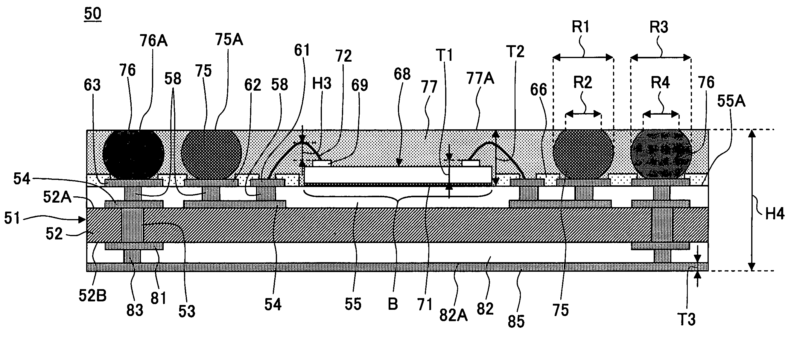
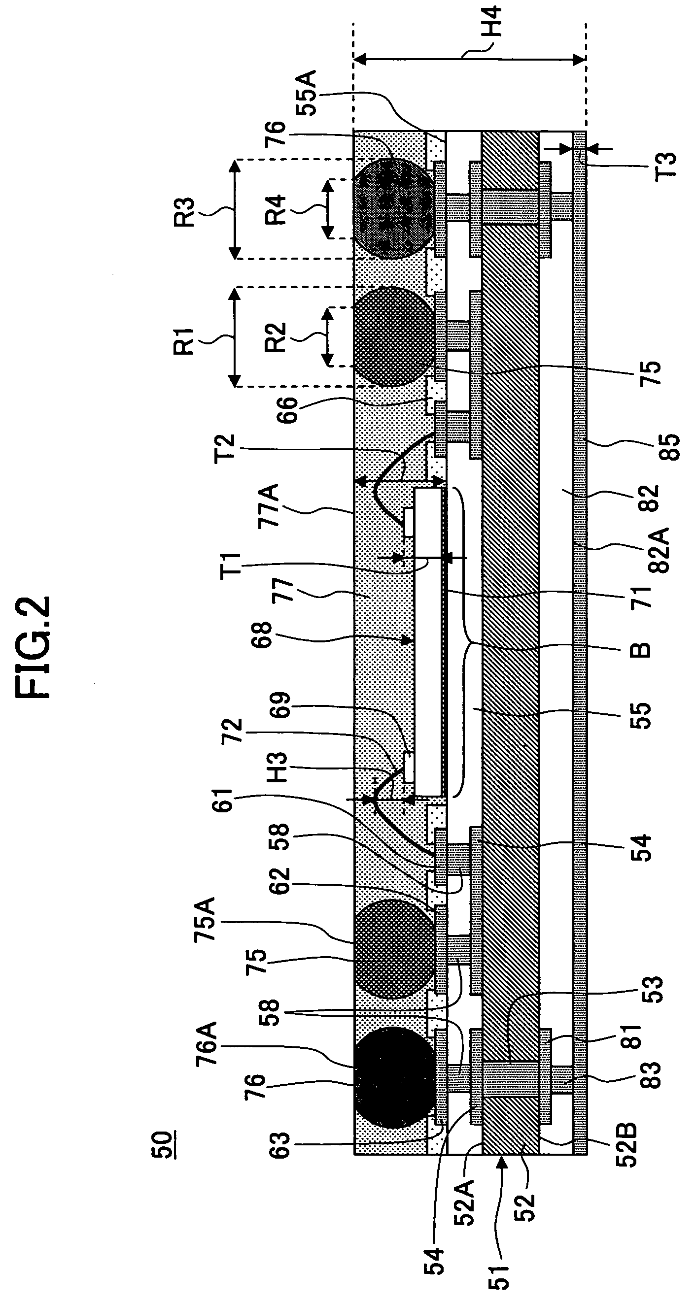
[0036]A semiconductor device 50 is described below with reference to FIGS. 2 and 3 according to a first embodiment of the present invention. FIG. 2 is a cross-sectional view illustrating the semiconductor device 50 according to the first embodiment of the present invention, wherein B represents an area on an upper resin layer 55 where a semiconductor chip 68 is mounted (hereinafter referred to as “chip mount area B”), H3 represents the height of wires 72 with reference to electrode pads 69 (hereinafter referred to as “height H3”), H4 represents the height of the semiconductor device 50 (hereinafter referred to as “height H4”), R1 represents the diameter of a generally spherical part of each connection terminal 75 (hereinafter referred to as “diameter R1”), R2 represents the diameter of a flat face 75A of each connection terminal 75 exposed from a transfer molded resin section 77 (hereinafter referred to as “diameter R2”), R3 represents the diameter of a generally spherical part of e...

second embodiment

[0060]A semiconductor device 100 is described below with reference to FIG. 9 according to a second embodiment of the present invention. FIG. 9 is a cross-sectional view illustrating the semiconductor device 100 according to the second embodiment of the present invention In FIG. 9, elements identical to those of the semiconductor device 50 shown in FIG. 2 are denoted by the same reference numerals. In FIG. 9, T5 represents the height of a shield member 107 (hereinafter referred to as “thickness. T5”).

[0061]The semiconductor device 100 generally comprises a board 101, a semiconductor chip 68, connection terminals 105, ground terminals 76, a transfer molded resin section 77, and the shield member 107.

[0062]The board 101 generally comprises a substrate 52, through vias 53, upper wiring portions 54, an upper resin layer 55, vias 58 and 83, wire connection portions 61, connection pads 63 and 104, solder resists 66 and 103, lower wiring portions 81, and a lower resin layer 82. The connecti...


PUM


Abstract

A semiconductor device is disclosed that comprises a board, a ground terminal disposed on the board, a connection terminal disposed on the board, a semiconductor chip mounted on the board, and a shield member electrically connected to the ground terminal. The semiconductor chip, the ground terminal, and the connection terminal are disposed on one side of the board, and the shield member is disposed directly on and covers the other side of the board.

Description

BACKGROUND OF THE INVENTION[0001]1. Field of the Invention[0002]The present invention generally relates to a semiconductor device, and particularly relates to a semiconductor device including a shield member.[0003]2. Description of the Related Art[0004]Semiconductor devices including shield cases for protecting electronic components mounted on boards from electromagnetic waves have been known in the art. FIG. 1 is a cross-sectional view illustrating a related-art semiconductor device 10 including a shield case 40, wherein H1 represents the height of a potting resin section 35 (hereinafter referred to as “height H1”), H2 represents the height of the semiconductor device 10 (hereinafter referred to as “height H2”), and A represents a clearance between the potting resin section 35 and the shield case 40 (hereinafter referred to as “clearance A”).[0005]With reference to FIG. 1, the semiconductor device 10 generally comprises a board 11, electronic components 26, a semiconductor chip 31,...

Claims


Application Information

Patent Timeline
Patent Type & Authority Patents(United States)
IPC IPC(8): H01R13/648H04B10/118
CPCH01L23/552H01R13/6594H01R13/6585H01R12/7076H01L2924/19105H01L2224/48227H01L2224/73265H01L2924/15331H01L2224/32225H01L2924/15321H01L2924/3025H01L2924/00012H01L2924/00H01L24/73H01L2924/181H01L2924/15192A45B9/04A45B1/00A63C11/227
Inventor AKAIKE, SADAKAZUINOUE, AKINOBUKAJIKI, ATSUNORITAKATSU, HIROYUKITSUBOTA, TAKASHIYAMANISHI, NORIO
Owner SHINKO ELECTRIC IND CO LTD
Why Eureka
Try Eureka