In-system programming of non-JTAG device using SPI and JTAG interfaces of FPGA device

a non-jtag device and in-system programming technology, applied in the field ofprogrammable devices, can solve the problems of increasing cost, requiring off-board programming, and occupying board space and fabrication costs

Active Publication Date: 2007-09-04
LATTICE SEMICON CORP
View PDF10 Cites 50 Cited by
  • Summary
  • Abstract
  • Description
  • Claims
  • Application Information

AI Technical Summary

Benefits of technology

[0009]In a further embodiment, the present invention provides a programmable device comprising (a) non-dedicated, programmable resources including programmable logic; (b) dedicated circuitry; (c) a Joint Test Action Group (JTAG) interface adapted to selectively interchange signals with the programmable logic via the dedicated circuitry; and (d) a Serial Peripheral Interface (SPI) adapted to (1) selectively interchange signals with the programmable logic via the dedicated circuitry and (2) selectively interchange signals with the JTAG interface via the dedicated circuitry, wherei

Problems solved by technology

However, most memory devices that are commonly used as boot PROMs do not comply with the JTAG standard and thus typically require off-board programming.
This approach involves the board space and fabrication cost of providing two different headers involving two different sets of operations.
The two-step approach for programming boot PROM 220 complicates the programming process, thereby increasing cost.
Further, programming an FPGA through a JTAG interface is costly in terms of vector

Method used


Image

  • In-system programming of non-JTAG device using SPI and JTAG interfaces of FPGA device
  • In-system programming of non-JTAG device using SPI and JTAG interfaces of FPGA device
  • In-system programming of non-JTAG device using SPI and JTAG interfaces of FPGA device

Examples


first embodiment

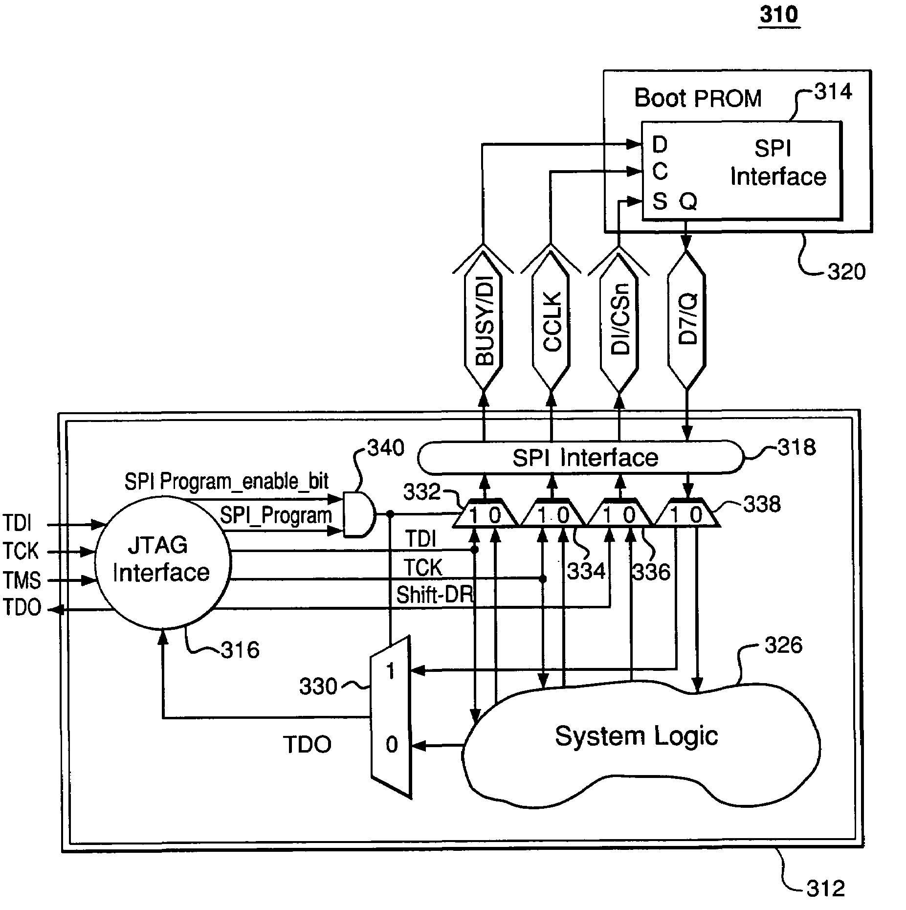
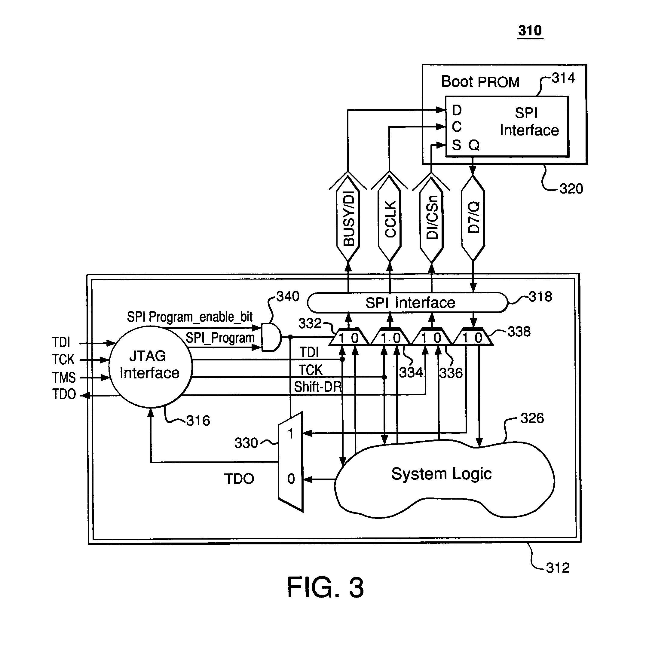
[0020]FIG. 3 shows a block diagram of an exemplary architecture 310 in the present invention, for using an FPGA 312 to program a JTAG-noncompliant boot PROM 320. As shown, in this exemplary embodiment, PROM 320 is a conventional SPI serial flash PROM device that includes a SPI interface 314. FPGA 312 includes a JTAG interface 316, a SPI interface 318, programmable system logic 326, a gate 340, four multiplexers (muxes) 330, 332, 334, 336, and a demultiplexer (demux) 338. JTAG interface 316 connects to a JTAG header (not shown) for attachment to an external JTAG-compliant device (not shown). JTAG interface 316 receives signals TDI, TCK, and TMS from the external device and provides a signal TDO to the external device, which signals are defined as follows:[0021]TDI: Test Data Input signal provided by the external device for supplying one or more of instructions and data from the external device to the registers of JTAG interface 316.[0022]TMS: Test Mode Select signal provided by the e...

second embodiment

[0085]FIG. 6 shows a block diagram of an exemplary architecture 610 in the present invention, for permitting multiple JTAG-noncompliant boot PROMs to be programmed in a daisy-chain formation using a plurality of FPGAs. As shown, this exemplary embodiment includes a JTAG chain of three FPGAs 612-1, 612-2, 612-3 connected to two boot PROMs 620-1, 620-2 at their respective SPI interfaces 614-1, 614-2. For ease of reference, the details of the JTAG and SPI ports of FPGAs 612-1, 612-2 are not shown, since such details are provided in FIG. 3 and its corresponding description above. FPGA 612-3 may be an FPGA consistent with the invention, as shown in FIG. 3, or may, alternatively, be a legacy or conventional FPGA, e.g., as shown in FIG. 1 or 2.

[0086]In this exemplary embodiment, FPGA 612-1 is used to program PROM 620-1, and FPGA 612-2 is used to program PROM 620-2. PROM 620-1 serves as the boot PROM for FPGA 612-1. PROM 620-2 is the boot PROM for both FPGAs 612-2 and 612-3, where FPGA 612-...


PUM


Abstract

A first programmable device comprises non-dedicated, programmable resources including programmable logic; dedicated circuitry; a Joint Test Action Group (JTAG) interface adapted to selectively interchange signals with the programmable logic via the dedicated circuitry; and a Serial Peripheral Interface (SPI) interface adapted to (1) selectively interchange signals with the programmable logic via the dedicated circuitry and (2) selectively interchange signals with the JTAG interface via the dedicated circuitry. The JTAG interface is adapted to be connected to a first external device. The SPI interface is adapted to be connected to a second external device. The first programmable device is adapted to transfer signals from the first external device to the second external device via the JTAG interface, the dedicated circuitry, and the SPI interface without relying on any of the programmable resources.

Description

TECHNICAL FIELD[0001]The present invention relates to programmable devices, such as field-programmable gate arrays (FPGAs), and, in particular, to techniques for programming certain devices, such as serial flash memory, that are non-compliant with Joint Test Action Group (JTAG) standards, by using the SPI (Serial Peripheral Interface) and JTAG interfaces of an FPGA device.BACKGROUND[0002]Volatile programmable devices, such as FPGAs, typically rely on non-volatile external storage media to hold the bitstreams used to configure the devices. For example, programmable read-only memory (PROM) devices are often used to hold the configuration bitstreams for FPGAs. Such devices are referred to as “boot PROMs,” because they are used to boot (i.e., initialize) programmable devices, such as volatile FPGAs. A boot PROM device is first programmed with a data pattern in the form of a bitstream corresponding to the desired FPGA configuration, which is typically achieved using an off-board stand-al...

Claims


Application Information

Patent Timeline
IPC IPC(8): H03K19/173G01R31/28
CPCG01R31/318516G01R31/318533H03K19/17748
Inventor TANG, HOWARDSINGH, SATWANTKOW, SAN-TA
Owner LATTICE SEMICON CORP
Why Eureka
Try Eureka