Semiconductor apparatus for monitoring critical path delay characteristics of a target circuit

a technology of critical path delay and mikroprocessor, which is applied in the field of mikroprocessor apparatus having monitor circuit, can solve the problems of increasing circuit scale, trade-off imbalance between delay monitoring accuracy and circuit, and achieve the effect of flexible and effective configuration

Inactive Publication Date: 2007-09-04
SONY CORP
View PDF2 Cites 10 Cited by
  • Summary
  • Abstract
  • Description
  • Claims
  • Application Information

AI Technical Summary

Benefits of technology

[0010]An object of the present invention is to provide a semiconductor apparatus by which a delay monitor c

Problems solved by technology

However, installation of a large number of delay circuits for dealing with the path switching leads to an increase of the cir

Method used


Image

  • Semiconductor apparatus for monitoring critical path delay characteristics of a target circuit
  • Semiconductor apparatus for monitoring critical path delay characteristics of a target circuit
  • Semiconductor apparatus for monitoring critical path delay characteristics of a target circuit

Examples


first embodiment

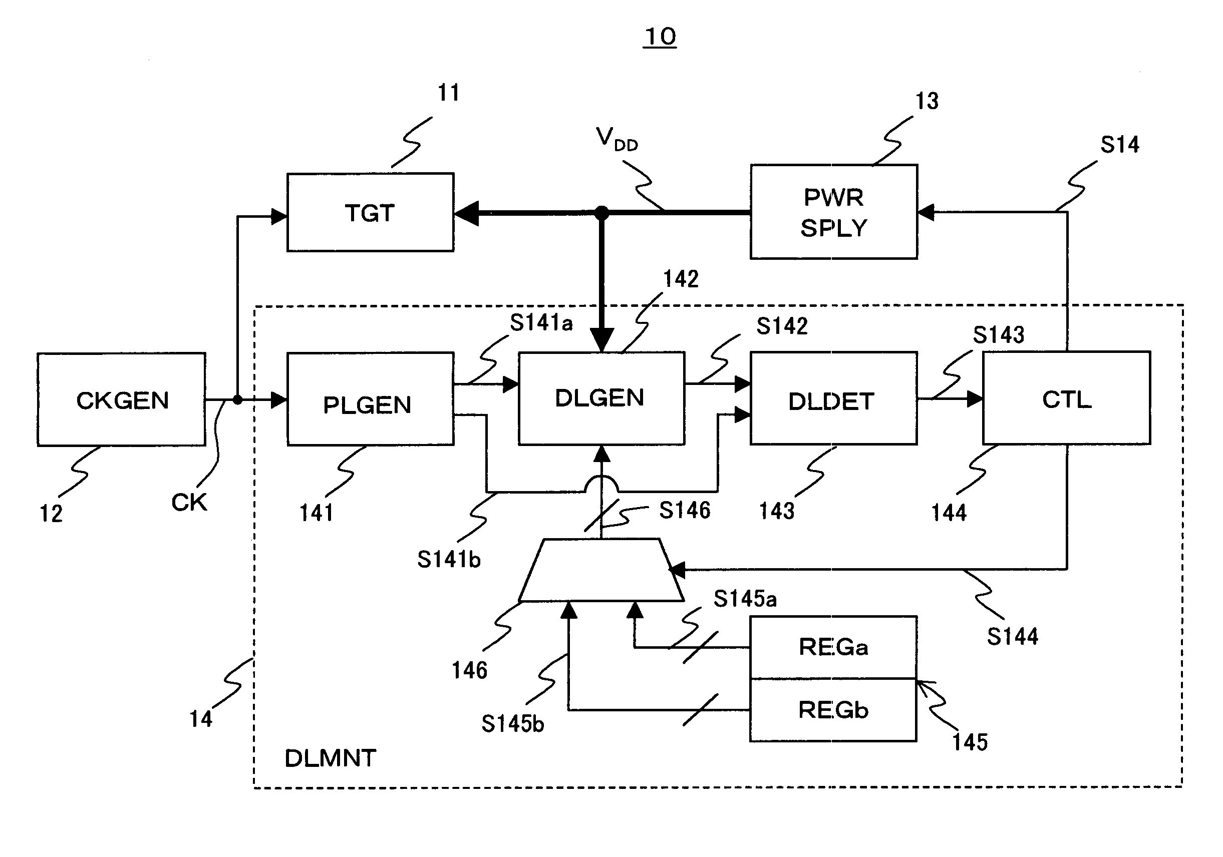
[0026]FIG. 1 is a block diagram of a first embodiment of a semiconductor apparatus according to the present invention.

[0027]The present semiconductor apparatus 10 comprises, as shown in FIG. 1, a target circuit (TGT) 11, a clock generation circuit (CKGEN) 12, a power source voltage supply circuit (PWRSPLY) 13 and a delay monitor circuit (DLMNT) 14.

[0028]The target circuit 11 comprises a semiconductor circuit (LSI) including a DSP, CPU or other logic circuits supplied with a power source voltage VDD from the power source voltage supply circuit 13 and operating in synchronization with a clock CK by the clock generation circuit 12.

[0029]The clock generation circuit 12 generates a clock CK having a predetermined frequency and supplies to the target circuit 11 and the delay monitor circuit 14.

[0030]The power source voltage supply circuit 13 receives a control signal S14 from the delay monitor circuit 14, adjusts the power source voltage VDD as instructed by the control signal, and suppli...

second embodiment

[0087]FIG. 6 is a block diagram of a second embodiment of a semiconductor apparatus according to the present invention.

[0088]A different point of the second embodiment from the above first embodiment is that a target circuit 11A comprises a circuit block operating at a plurality of different frequencies.

[0089]For example, when a CPU operates at a clock frequency of f1 and a DSP operates at a clock frequency of f2 in an LSI installed with the CPU and the DSP, there is no telling that a circuit of which frequency domain becomes a critical path for the target circuit 11A depending on conditions of an operation voltage and temperature, etc.

[0090]Accordingly, it is necessary that the delay monitor circuit 14A monitor delay of the circuits respectively operating at the clock frequency of f1 and clock frequency of f2.

[0091]A clock generation circuit 12A according to the present second embodiment generates a clock CK1 of a frequency f1 and a clock CK2 of a frequency f2 and supplies to the t...


PUM


Abstract

A semiconductor apparatus for flexibly and effectively configuring a delay monitor circuit without an increase in circuit scale includes a delay signal generation circuit for switching the configuration of delay element arrays based on first configuration information and second configuration information and propagating a delay element array wherein a pulse is switched, a register group having a first register for the first configuration information and a second register for second configuration information, a selector for outputting to the delay signal generation circuit the first configuration information and second configuration information in accordance with an instruction of a selection signal in a time sharing way, and a control circuit for controlling a power source voltage based on delay information of a delay element array and outputting to the selector a selection signal to select from the first configuration information and second configuration information in a time sharing way.

Description

BACKGROUND OF THE INVENTION[0001]1. Field of the Invention[0002]The present invention relates to a semiconductor apparatus having a monitor circuit for perceiving critical path delay characteristics of a target circuit, and particularly relates to a technique of attaining a low power consumption by adaptively controlling a power source voltage supplied to an LSI as the target circuit.[0003]2. Description of the Related Art[0004]In recent years, a method of lowering a power source voltage for attaining a low power consumption has been generally used in a semiconductor circuit. This is because AC components of a power consumption of a semiconductor circuit (LSI) is proportional to a square of a power source voltage, and a reduction of the power source voltage is the most effective for lowering a power consumption of the LSI.[0005]From such a viewpoint, in recent years, there has been reported a method for adaptively supplying a minimum voltage for operating an LSI by dynamically contr...

Claims


Application Information

Patent Timeline
IPC IPC(8): H03K5/19H01L27/04H01L21/822H03H11/26H03K5/00H03K5/131H03K5/14H03L7/081
CPCH03L7/0805H03L7/0814H03K2005/00058
Inventor SEKI, TAKAHIRONAKAI, MASAKATSUMEGURO, TETSUMASA
Owner SONY CORP
Why Eureka
Try Eureka