Method for measuring offset voltage of sense amplifier and semiconductor employing the method

a technology of sense amplifier and offset voltage, which is applied in the direction of information storage, static storage, digital storage, etc., can solve the problems of difficult calculation of the pure offset voltage of the bit line sense amp, inability to ensure the stable operation of the semiconductor memory device, and difficulty in precisely measuring the capacitance of the unit cell in the cell array and the capacitance of the bit line coupled to the unit cell

Active Publication Date: 2007-09-04
SK HYNIX INC
View PDF18 Cites 29 Cited by
  • Summary
  • Abstract
  • Description
  • Claims
  • Application Information

AI Technical Summary

Benefits of technology

[0014]The invention provides a semiconductor memory device that computes the offset voltage of a bit line sense amp, by supplying a controllable test voltage to a bit line sense amp.
[0014]The invention provides a semiconductor memory device that computes the offset voltage of a bit line sense amp, by supplying a controllable test voltage to a bit line sense amp.

Problems solved by technology

In the conventional method, however, it is troublesome to precisely measure the capacitance of a unit cell in the cell array and the capacitance of the bit line coupled to the unit cell.
Calculation of the pure offset voltage of the bit line sense amp has been difficult and until now, this voltage has been approximately calculated rather than actually measured.
Stable operation of a semiconductor memory device cannot be guaranteed unless the offset voltage is correct.

Method used


Image

  • Method for measuring offset voltage of sense amplifier and semiconductor employing the method
  • Method for measuring offset voltage of sense amplifier and semiconductor employing the method
  • Method for measuring offset voltage of sense amplifier and semiconductor employing the method

Examples


Embodiment Construction

[0039]Hereinafter, an exemplary semiconductor memory device according to the invention is described in detail with reference to the accompanying drawings.

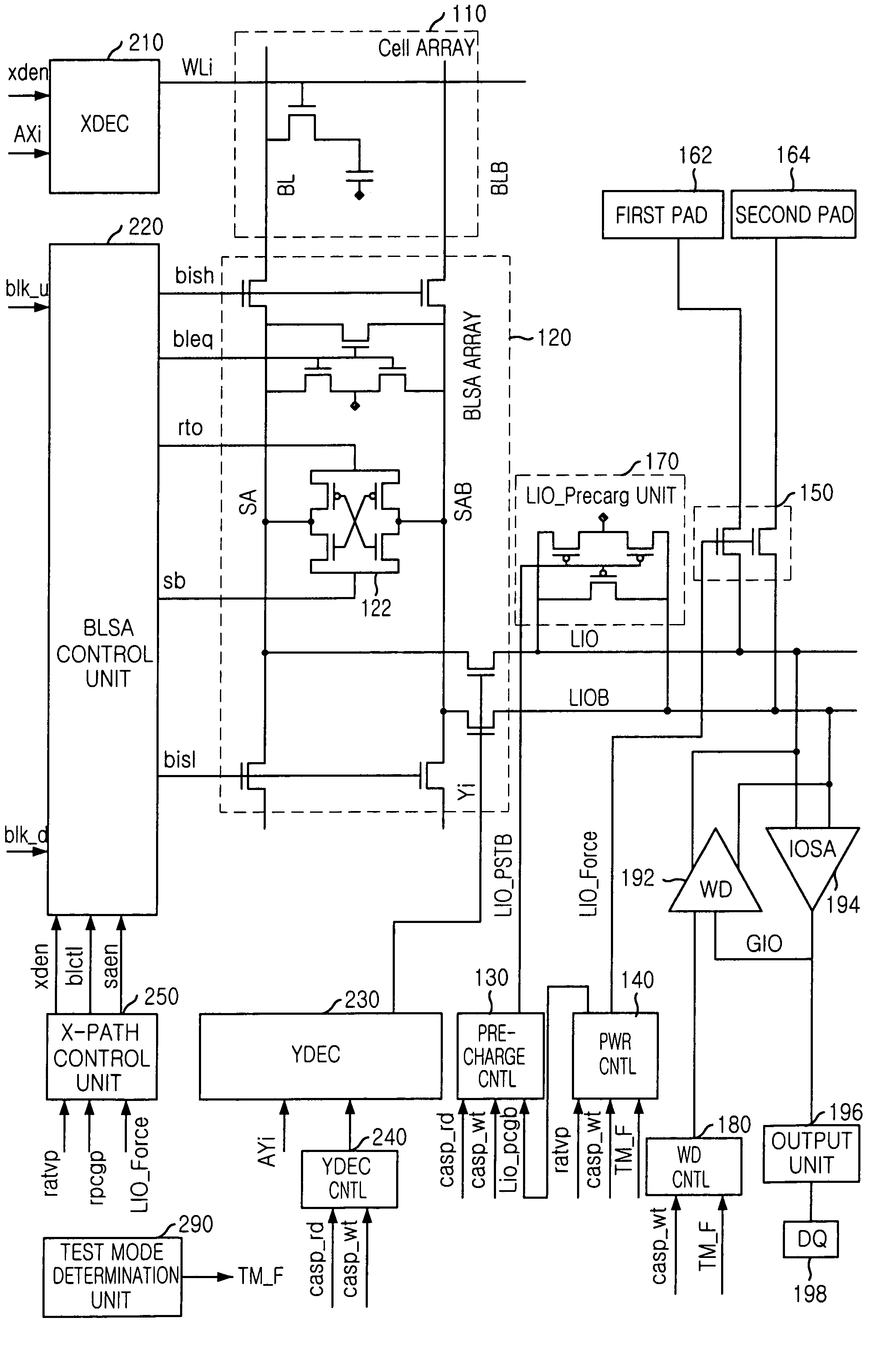
[0040]FIG. 3 is a block diagram showing the configuration of data input / output paths in a semiconductor memory device in accordance with an exemplary embodiment of the present invention.

[0041]As shown, the semiconductor memory device includes a bit line sense amp block 120 having a bit line sense amp 122 for amplifying the voltage difference between a bit line BL and an inversion bit line BLB which convey data written in a memory cell array 110 upon reading the data; a local input / output line LIO and an inversion local input / output line LIOB within a core region that are coupled to the bit line and the inversion bit line by one or more switches; a first external voltage supply pad 162 connected to local input / output line LIO; a second external voltage supply pad 164 connected to the inversion local input / output line LIOB; and an ex...


PUM


Abstract

A semiconductor memory device precisely measures the offset voltage of a bit line sense amplifier. The semiconductor memory device of the invention includes: a bit line sense amplifier for amplifying a voltage difference between a bit line and an inversion bit line, which carry data written on a memory cell when the data is read; a data input / output line and an inversion data input / output line within a core region coupled to the bit line and the inversion bit line via one or more switches; a first external voltage supply pad connected to the data input / output line; a second external voltage supply pad connected to the inversion data input / output line; and an external voltage supply controller for switching a connection of the data input / output line and the first external voltage supply pad and a connection of the inversion data input / output line and the second external voltage supply pad.

Description

CROSS-REFERENCES TO RELATED APPLICATIONS[0001]This application claims priority to Korean Patent Application No. 10-2004-0087670, filed Oct. 30, 2004, of Chang-Ho Do et al., titled “Semiconductor Memory Device and Bit Line Sense Amplifier Offset Voltage Measuring Method of It,” which is incorporated by reference herein in its entirety for all purposes.BACKGROUND OF THE INVENTION[0002]The present invention relates to semiconductor memory devices; and, more particularly, to semiconductor memory devices that measure the offset voltage of sense amplifiers.[0003]In a semiconductor memory device such as a dynamic random access memory (DRAM), a bit line sense amplifier (hereinafter, “amp”) is used to amplify a low voltage level of data stored in each memory cell so that the data can be read outside the memory device.[0004]FIG. 1 shows a data read path and a data write path in a core region of a conventional semiconductor memory device.[0005]As shown, the memory device includes a cell array ...

Claims


Application Information

Patent Timeline
Patent Type & Authority Patents(United States)
IPC IPC(8): G11C7/02
CPCG11C7/065G11C7/1048G11C29/02G11C29/026G11C2029/5004G11C2207/002G11C2207/105G11C7/06G11C7/08
Inventor DO, CHANG-HOSON, JIN-SEOK
Owner SK HYNIX INC
Why Eureka
Try Eureka