Optoelectronic component

a technology of optoelectronic components and components, applied in the direction of semiconductor devices, semiconductor/solid-state device details, electrical apparatus, etc., can solve the problem of increasing the risk of component failure after soldering

Active Publication Date: 2007-09-18
OSRAM OLED
View PDF15 Cites 26 Cited by
  • Summary
  • Abstract
  • Description
  • Claims
  • Application Information

AI Technical Summary

Benefits of technology

[0007]This increases the risk of failure of the component after soldering, the cause of which can frequently be traced to severing of the electrical or mechanical connection between the chip carrier and the chip. Even the slightest warming of the component can lead to an open electrical contact between the chip and the chip carrier.
[0008]It is, therefore, an object of the present invention to provide a component of the above-cited kind whose reliability is increased.

Problems solved by technology

This increases the risk of failure of the component after soldering, the cause of which can frequently be traced to severing of the electrical or mechanical connection between the chip carrier and the chip.

Method used


Image

  • Optoelectronic component
  • Optoelectronic component
  • Optoelectronic component

Examples


Embodiment Construction

[0039]Concerning the figures, it should be noted that like reference numerals denote elements that are the same or at least perform like or similar functions.

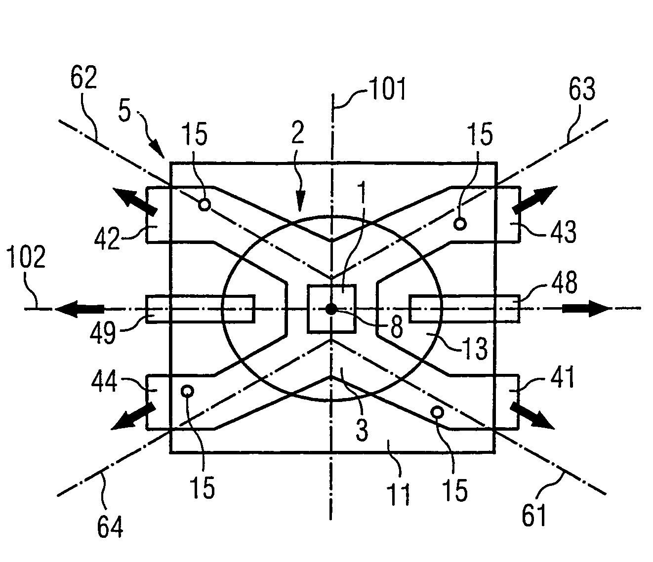
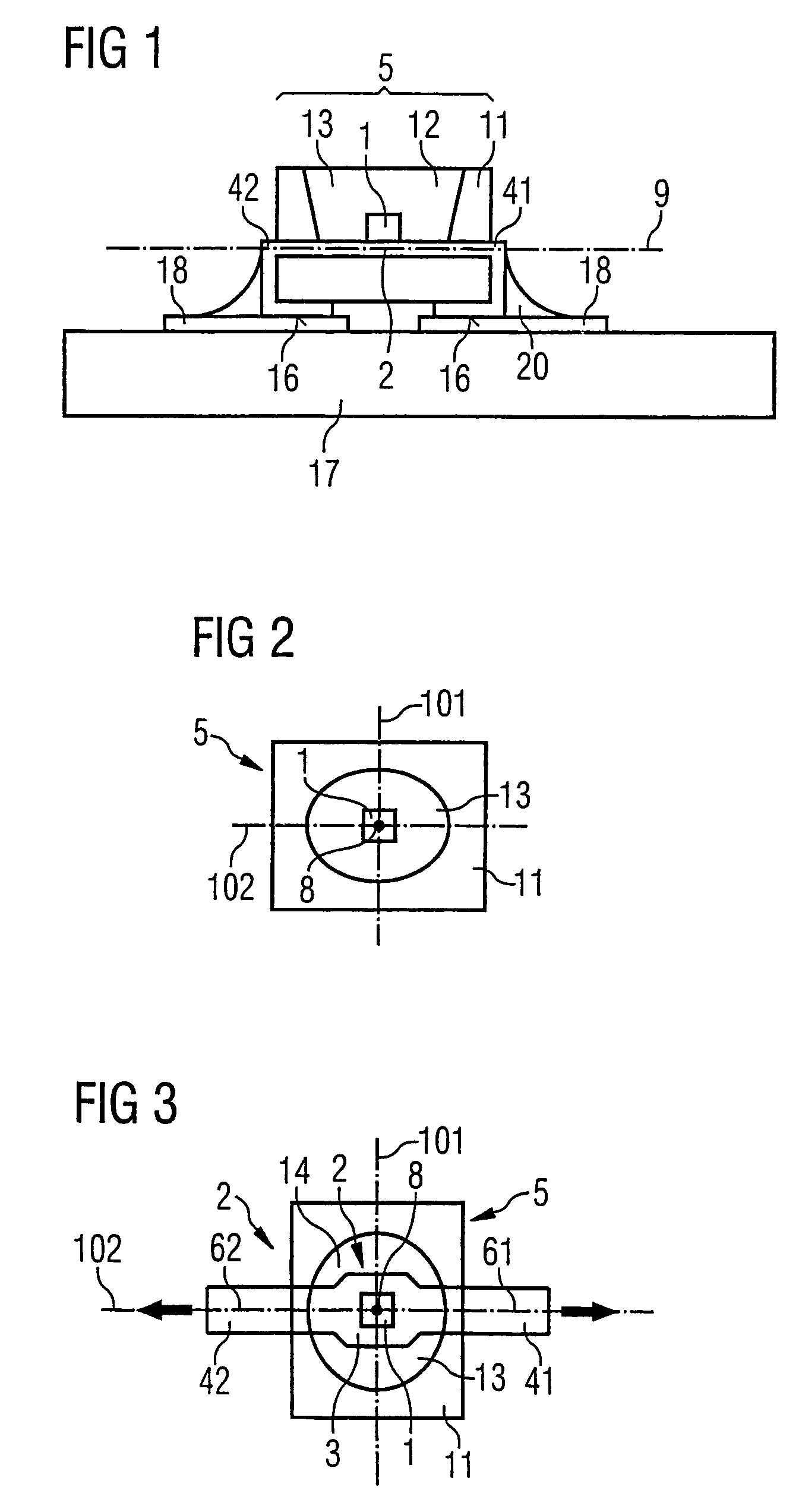
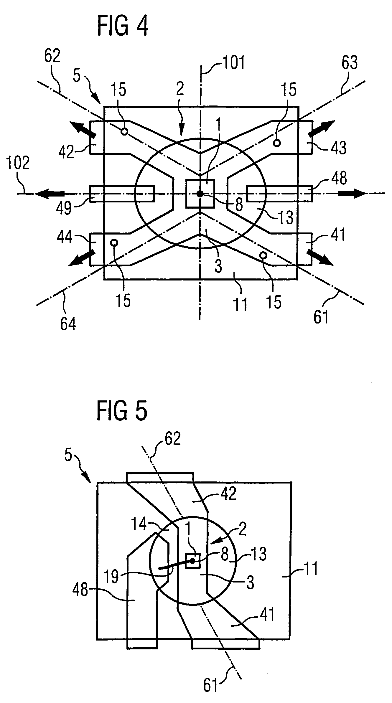
[0040]FIG. 1 depicts a component comprising an optoelectronic chip 1 that is fixed on a chip carrier 2. Said optoelectronic chip 1 can, for example, be a light-emitting diode, or it can instead be a laser diode. The optoelectronic chip 1 can radiate vertically or laterally. In the latter case, the housing 11 is shaped so that the inner sides of the recess 12 form a reflector for the light radiated by the chip 1.

[0041]The chip carrier 2 can be made from a leadframe, for example. This has the advantage of enabling a large run of components to be produced simply and inexpensively. In this case, chip carrier 2 is made from a very thin, conductive metal sheet out of which a specific shape is stamped. For example, an iron / nickel alloy can be considered for use as the material of the chip carrier 2.

[0042]Chip 1 and the central portion...


PUM


Abstract

The invention relates to an optoelectronic component containing an optoelectronic chip (1) and containing a chip carrier (2) that has a central region (3) on which the chip is fixed and that comprises terminals (41, 42, 43, 44) extending outwardly from the central region of the chip carrier (2) to the outside, wherein the chip and portions of the chip carrier are enveloped by a body (5) and wherein the projection of the body and that of each of the longitudinal axes of the terminals onto the contact plane between the chip and the chip carrier are substantially point-symmetrical with respect to the central point of the chip. The invention further relates to an arrangement comprising said component. The advantage of the symmetrical configuration of the component is that the risk of thermomechanically induced failures of the component is reduced.

Description

CROSS-REFERENCE TO RELATED APPLICATIONS[0001]This application is the National Stage of International Application No. PCT / DE2003 / 003923, filed Nov. 27, 2003, which claims the benefit of German Patent Applications Serial No. 10255932.5, filed on Nov. 29, 2002 The contents of both applications are hereby incorporated by reference in their entireties.FIELD OF THE INVENTION[0002]The invention relates to an optoelectronic component comprising an optoelectronic chip, a chip carrier, and a housing.BACKGROUND OF INVENTION[0003]Components of the aforesaid kind are known, for example, from the document WO 99 / 07023. In these components, an optoelectronic chip is fixed on a chip carrier. The chip and portions of the chip carrier are surrounded by and embedded in a housing. The housing can be fabricated by injection overmolding. The chip carrier has a region on which the optoelectronic chip is fixed. The chip carrier also has terminals that run from the chip-carrying region outwardly out of the h...

Claims


Application Information

Patent Timeline
Patent Type & Authority Patents(United States)
IPC IPC(8): H01L29/22H01L33/48H01L33/62
CPCH01L33/62H01L33/486H01L2224/48247H01L2224/48465H01L2924/00
Inventor ARNDT, KARLHEINZBOGNER, GEORGWAITL, GUNTERWINTER, MATTHIAS
Owner OSRAM OLED
Why Eureka
Try Eureka