Semiconductor memory device and method of manufacturing the same
a memory device and semiconductor technology, applied in the direction of transistors, solid-state devices, instruments, etc., can solve the problems of increasing the power consumption of an sram, difficult to apply dtmos to a device required, and further difficult to apply dtmos to a device, so as to reduce the increase of power consumption, improve the reliability of operation, and suppress the increase of an area
- Summary
- Abstract
- Description
- Claims
- Application Information
AI Technical Summary
Benefits of technology
Problems solved by technology
Method used
Image
Examples
first preferred embodiment
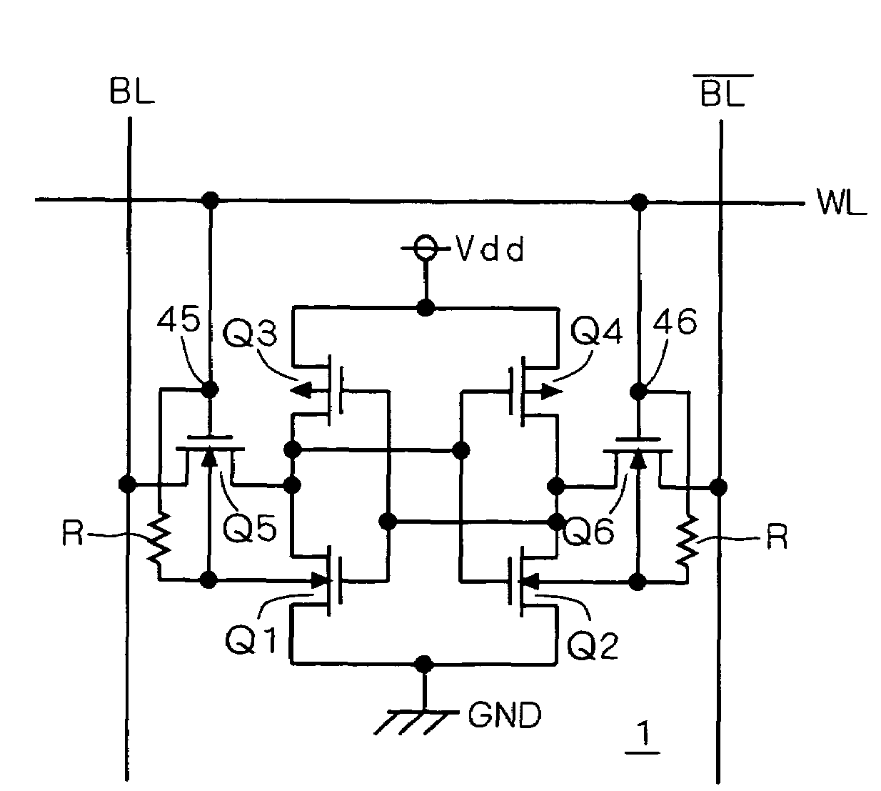
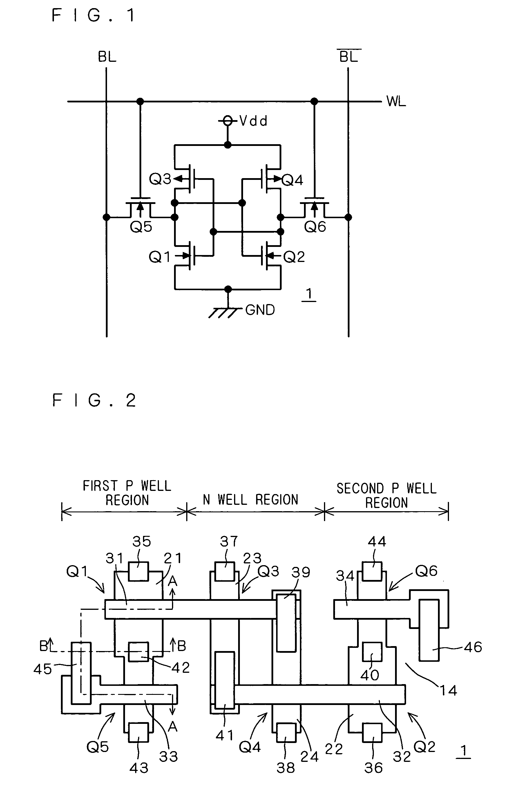
[0056]FIG. 1 is a circuit diagram of each memory cell (SRAM cell) 1 of a general SRAM. As shown in FIG. 1, first and second driver transistors Q1 and Q2 which are driving NMOS transistors (driver MOS transistors) and first and second load transistors Q3 and Q4 which are load PMOS transistors (load MOS transistors) constitute a pair of inverters. These inverters are interconnected with each other to constitute a flip-flop circuit. This flip-flop circuit and first and second access transistors Q5 and Q6 which are data transfer NMOS transistors (access MOS transistors) constitute the SRAM cell 1. The gates of the access transistors Q5 and Q6 are connected to a word line WL, while the sources / drains of the access transistors Q5 and Q6 are connected to bit lines BL and / BL respectively.
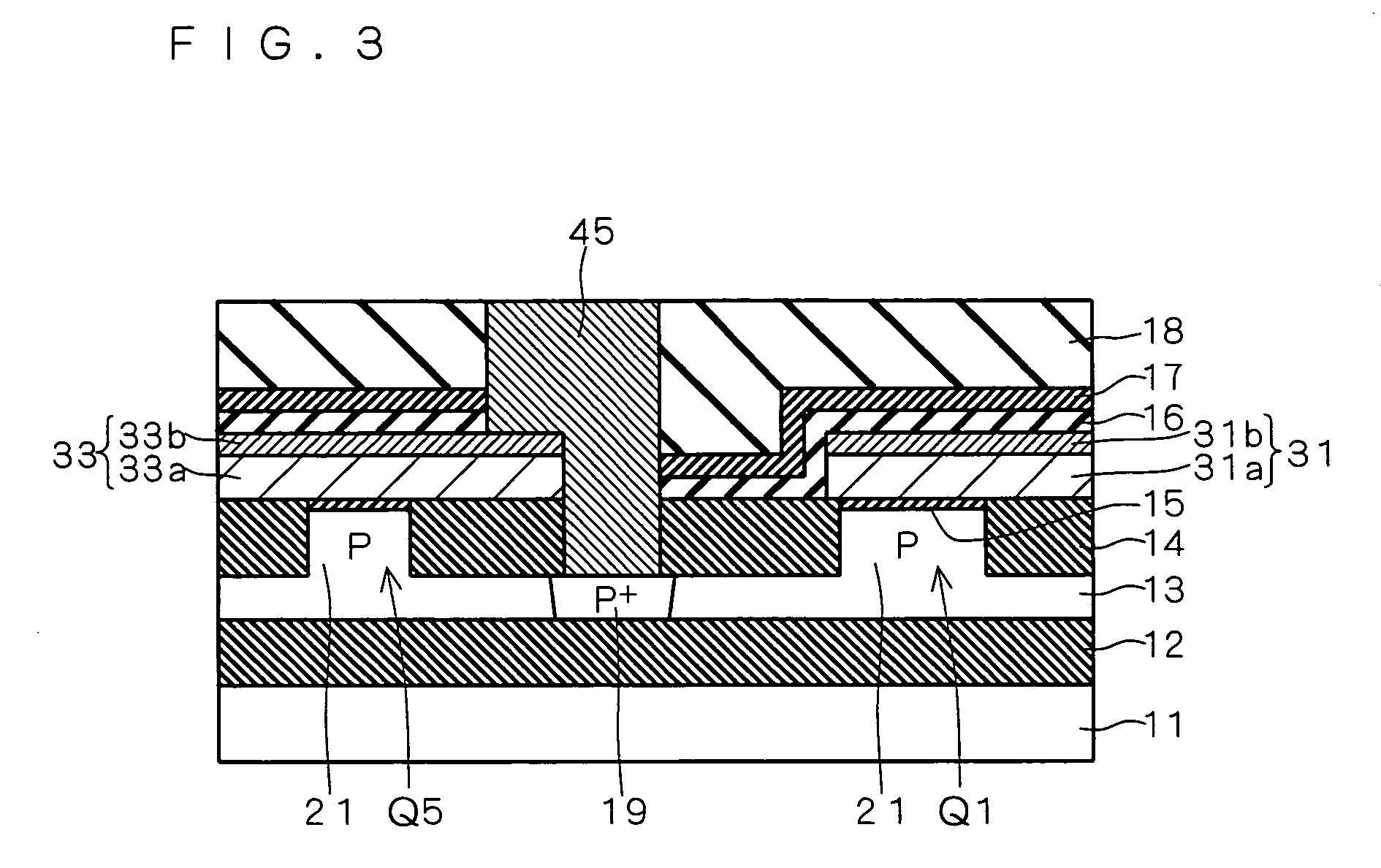
[0057]FIG. 2 is a top plan view of each memory cell 1 of an SRAM forming a semiconductor memory device according to a first preferred embodiment of the present invention. As shown in FIG. 2, the SRAM cell ...
second preferred embodiment
[0089]FIG. 17 is a top plan view of an SRAM cell 1 according to a second preferred embodiment of the present invention. Referring to FIG. 17, elements having functions similar to those of the elements shown in FIG. 2 are denoted by the same reference numerals, to omit redundant description. Also in the second preferred embodiment, a group of a first driver transistor Q1, a first load transistor Q3 and a first access transistor Q5 and a group of a second driver transistor Q2, a second load transistor Q4 and a second access transistor Q6 are similar in structure to each other.
[0090]Similarly to the first preferred embodiment, a contact 45 is electrically connected to body regions of the first access transistor Q5 and the first driver transistor Q1 and a contact 46 is electrically connected to body regions of the second driver transistor Q2 and the second access transistor Q6 also in the SRAM cell 1 according to the first preferred embodiment. In other words, FIG. 55 also corresponds t...
third preferred embodiment
[0109]In an SRAM cell 1 according to a third preferred embodiment of the present invention, the DTMOS technique is applied to load transistors Q3 and Q4. FIG. 28 is a top plan view of the SRAM cell 1 according to the third preferred embodiment. Also referring to FIG. 28, elements having functions similar to those of the elements shown in FIG. 2 are denoted by the same reference numerals. The SRAM cell 1 according to the third preferred embodiment has an N-type seventh active region 67 joined to a third active region 23 and an N-type eighth active region 68 joined to a fourth active region 24. The seventh and eighth active regions 67 and 68 are N+ regions having higher impurity concentrations than the remaining portions of the remaining N well regions.
[0110]FIGS. 29A and 29B are sectional views of a second load transistor Q4 in the SRAM cell 1 taken along the lines E-E and F-F in FIG. 28 respectively. A first load transistor Q3 is similar in structure to the second load transistor Q4...
PUM
 Abstract
Description
Claims
Application Information


