
Apparatus and method for cooling semiconductor devices

a semiconductor device and apparatus technology, applied in the field of integrated circuits, can solve the problems of affecting the operation of the device, the minimum limit may be too large to accommodate the trend towards smaller devices, and the negative increase of the die siz

Active Publication Date: 2007-09-25
NVIDIA CORP
View PDF7 Cites 11 Cited by
  • Summary
  • Abstract
  • Description
  • Claims
  • Application Information

AI Technical Summary

Benefits of technology

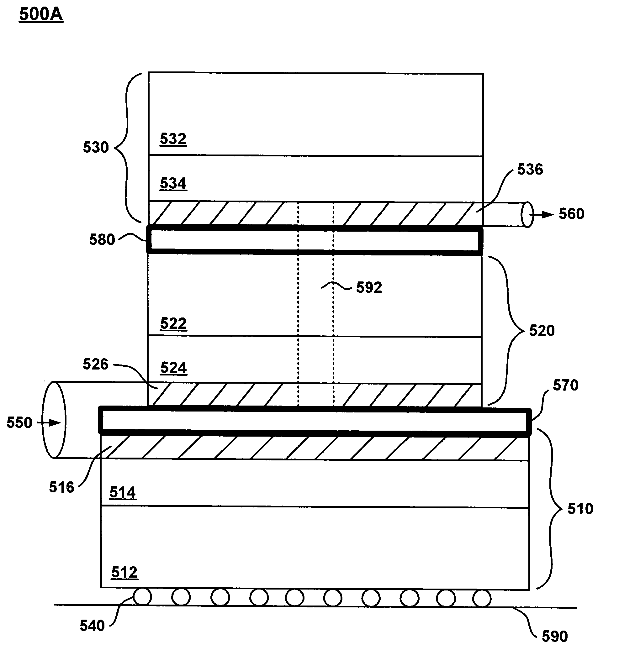
[0011]Accordingly, various embodiments of the present invention disclose an apparatus and method for cooling semiconductor devices. As a result, embodiments of the present invention are capable of cooling the higher density dies by incorporating a cooling system within the semiconductor substrate of the die itself. In addition, by incorporating the cooling mechanism within the semiconductor substrate of the die, proper cooling of dies within a stacked die configuration is maintained.

Problems solved by technology

However, fans require battery power for operation which is problematic for battery operated devices.
This minimum limit may be too large to accommodate the trend towards smaller devices.
In either case, the attached heat sinks negatively increase the size of the die.
This in turn increases the size of the electronic device incorporating the die and the attached heat sink.
In addition, these traditional systems and methods provide limited cooling of stacked die configurations.
However, in a stacked die configuration, exposed surface area of the die is significantly reduced, thereby reducing the effectiveness of active cooling systems incorporating the circulation of air.
For example, the middle die in a three die stacked die configuration has very limited surface area for dissipating heat.
Also, attaching a heat sink to the top of a die stacked configuration only effectively cools the uppermost die of the stacked die configuration, resulting in limited or no cooling of the lower die in the stacked die configuration.
As a result, traditional cooling systems and cooling methods for integrated circuits provide limited cooling as the density of components increases on dies, either through the shrinkage in size of the electrical components, or through a combination of component shrinkage and the placement of dies in a stacked die configuration.

Method used


Image

  • Apparatus and method for cooling semiconductor devices
  • Apparatus and method for cooling semiconductor devices
  • Apparatus and method for cooling semiconductor devices

Examples


Embodiment Construction

[0026]Reference will now be made in detail to the preferred embodiments of the present invention, an apparatus and method for cooling semiconductor devices, examples of which are illustrated in the accompanying drawings. While the invention will be described in conjunction with the preferred embodiments, it will be understood that they are not intended to limit the invention to these embodiments. On the contrary, the invention is intended to cover alternatives, modifications and equivalents, which may be included within the spirit and scope of the invention as defined by the appended claims.

[0027]Furthermore, in the following detailed description of the present invention, numerous specific details are set forth in order to provide a thorough understanding of the present invention. However, it will be recognized by one of ordinary skill in the art that the present invention may be practiced without these specific details. In other instances, well known methods, procedures, components...


PUM

PropertyMeasurementUnit
aspect ratioaaaaaaaaaa
thermal energyaaaaaaaaaa

Abstract

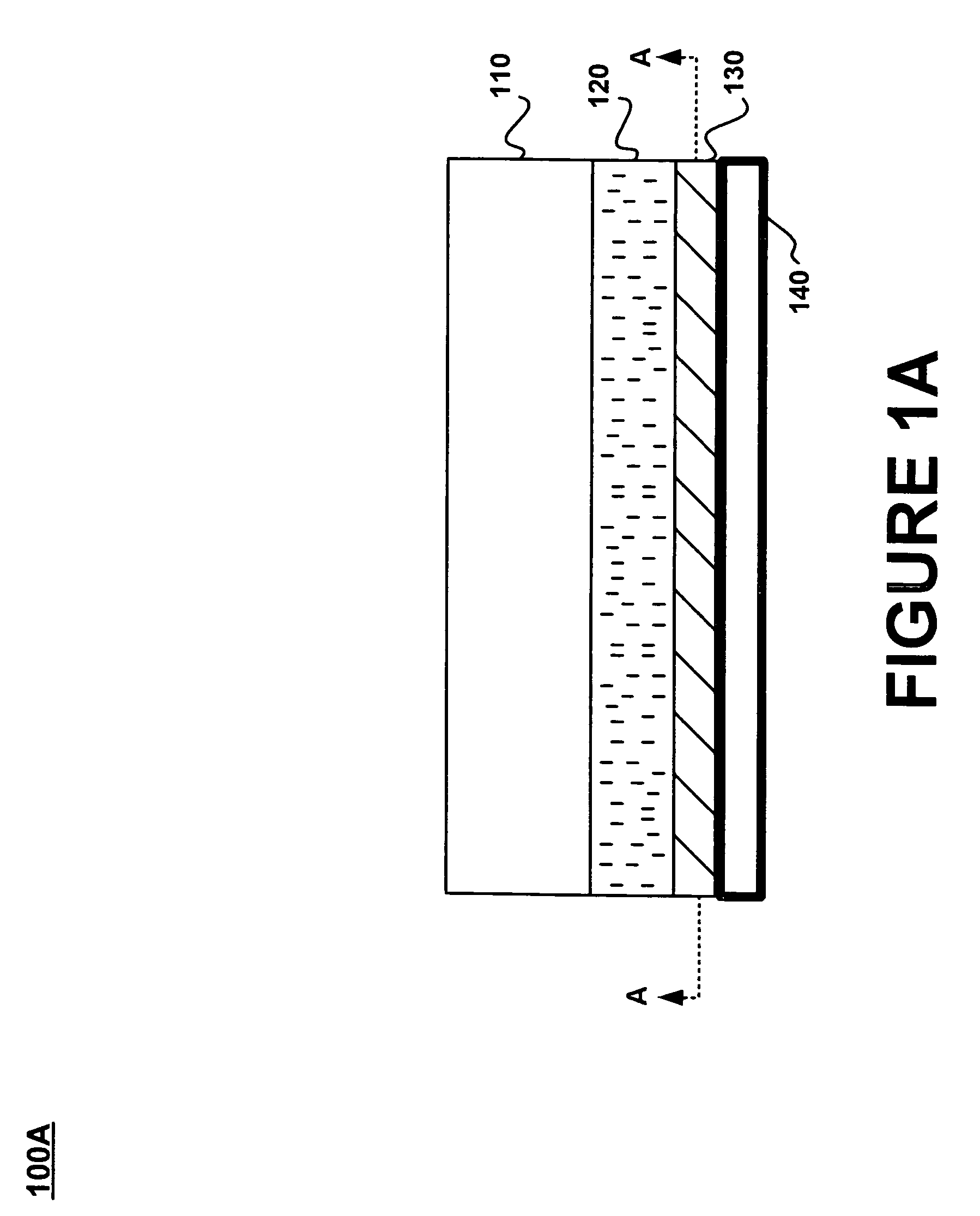
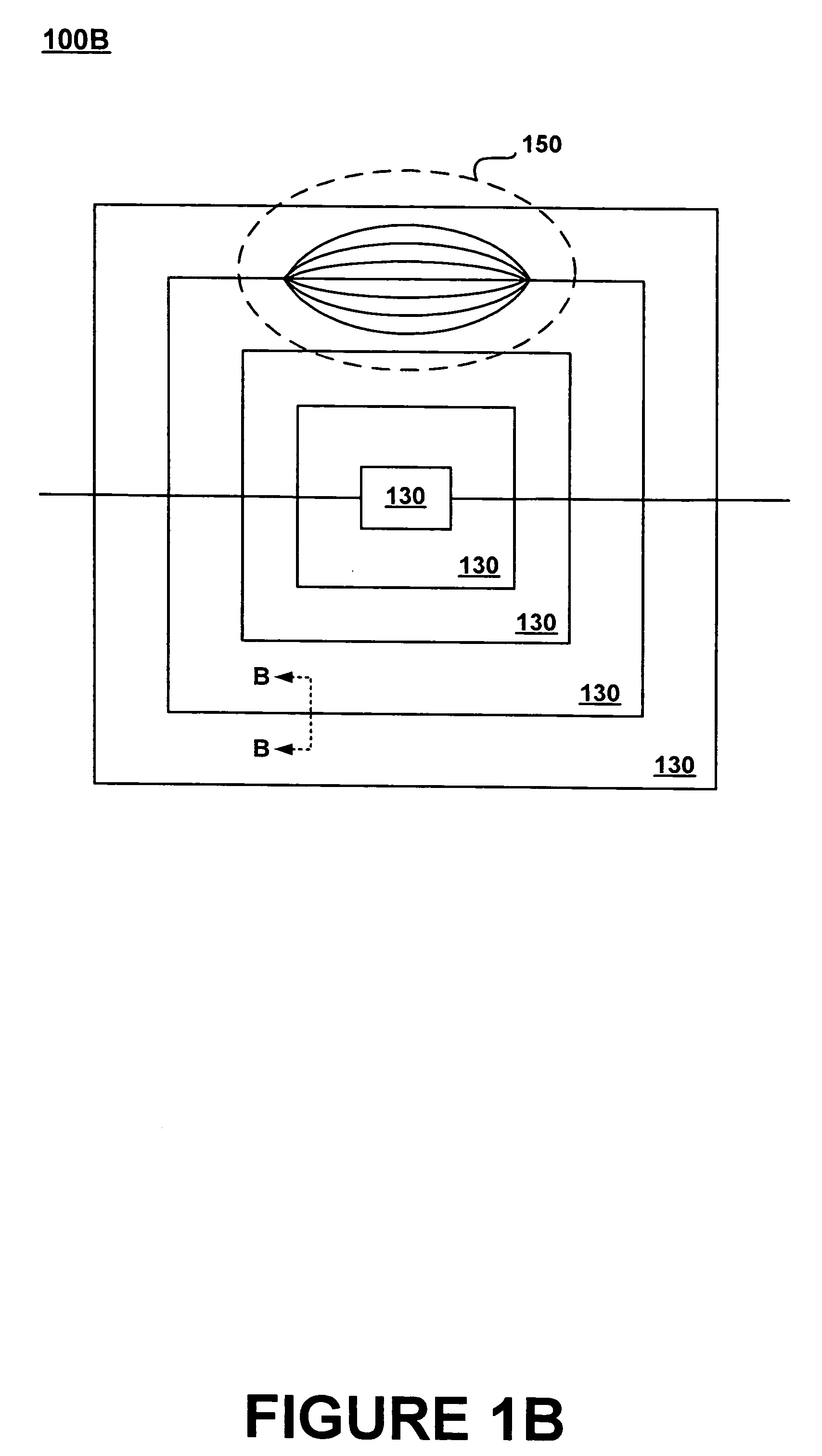
An apparatus and method for cooling semiconductor devices. A cooling system for semiconductor devices is disclosed and includes a semiconductor substrate, horizontal channels and a cooling medium. Specifically, the semiconductor substrate is incorporated into a die. Also, one or more horizontal channels are formed in a backside of the semiconductor substrate of the die. The horizontal channels collect thermal energy that is generated by electrical components located on a front side of the semiconductor substrate. A cooling medium circulates within the one or more horizontal channels for transferring the thermal energy away from the die.

Description

CROSS REFERENCE TO RELATED APPLICATION[0001]This patent application claims priority and is a Divisional of co-pending, commonly-owned patent application Ser. No. 10 / 853,432, filed on May 24, 2004, entitled “Apparatus and Method for Cooling Semiconductor Devices”, by Ira Chayut, and assigned to the assignee of the present invention, the disclosure of which is incorporated herein by reference.BACKGROUND OF THE INVENTION[0002]1. Field of the Invention[0003]Embodiments of the present invention relate to the field of integrated circuits. More particularly, embodiments of the present invention relate generally to cooling systems for transferring thermal energy away from integrated circuits.[0004]2. Related Art[0005]The trend in decreasing the size of semiconductor components leads to smaller electronic devices that are computationally more powerful than their older counterparts. For example, mobile devices, such as cell phones and personal digital assistants, are packed with multiple func...

Claims


Application Information

Patent Timeline
Patent Type & Authority Patents(United States)
IPC IPC(8): H05K7/20B23P15/00F28F7/00H01L23/34
CPCH01L23/473H01L25/0657Y10T29/49359H01L2224/73253H01L2225/06589H01L2224/16
Inventor CHAYUT, IRA G.
Owner NVIDIA CORP
Learn More