
Bi-directional deflectable resistor

a resistor and bi-directional technology, applied in the field of deflectable resistors, can solve the problems of micro-cracks, open and separate, and large number of micro-cracks

Active Publication Date: 2007-10-02
SENSITRON INC
View PDF10 Cites 24 Cited by
  • Summary
  • Abstract
  • Description
  • Claims
  • Application Information

AI Technical Summary

Benefits of technology

"The present invention provides a bi-directional deflectable resistor that can bend in multiple directions and predictably change resistance when bended. The resistor includes a substrate, first and second layers of conductive material, and first and second layers of resistive ink. The substrate can bend from a first configuration to a second configuration and from a first direction to a second direction, and the resistance of the first and second layers of conductive ink changes predictably when bended in the first direction and the second direction. The first and second layers of resistive ink are deposited on the substrate in spaced apart segments. The invention also includes connector means for interconnection to external electrical components. The technical effects of the invention include improved flexibility, durability, and accuracy of resistance measurement for bending sensors."

Problems solved by technology

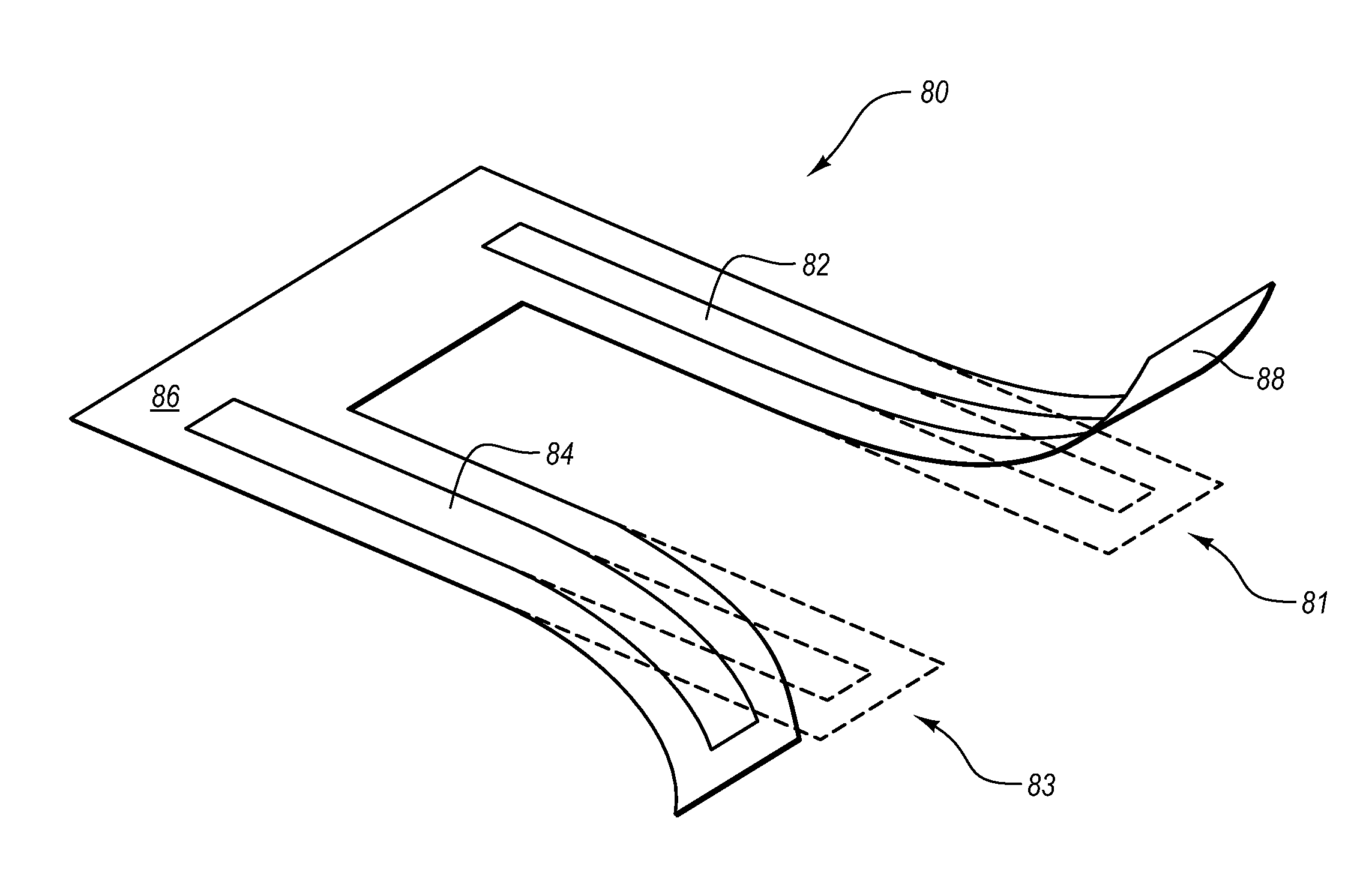
In operation, the bending of the first layer of conductive material between the first configuration and the second configuration causes a number of micro-cracks that are added during the manufacturing process to open up and separate in the first layer of conductive material.
Similarly, the bending of said second layer of conductive material between the first configuration and the third configuration causes a number of micro-cracks that are added during the manufacturing process to open up and separate in said second layer of conductive material.

Method used


Image

  • Bi-directional deflectable resistor
  • Bi-directional deflectable resistor
  • Bi-directional deflectable resistor

Examples


Embodiment Construction

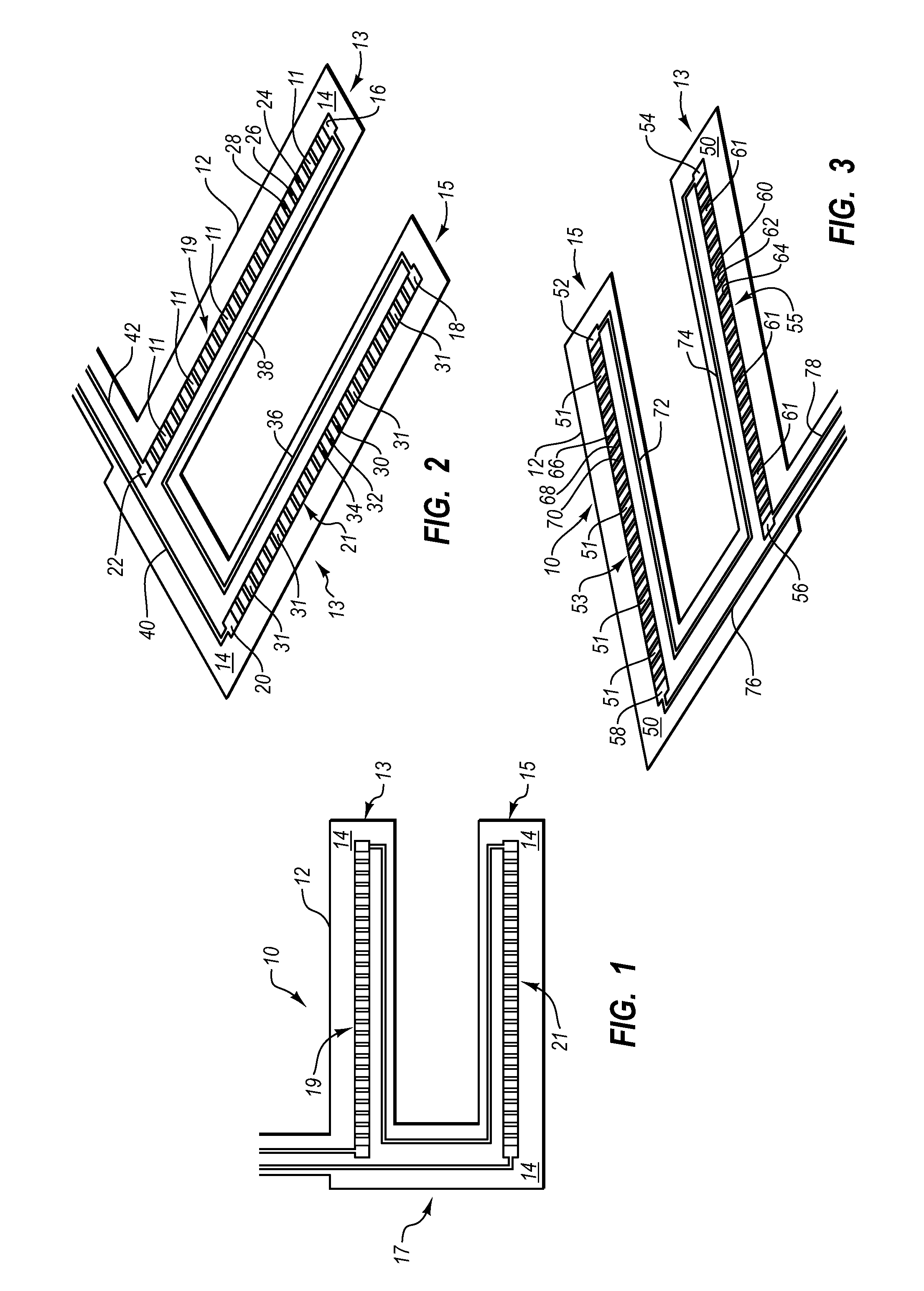
[0030]FIG. 1 illustrates a top view of a bi-directional deflectable resistor 10. Bi-directional deflectable resistor 10 comprises a substrate 12 that is double sided, thereby having both a top surface 14 and a bottom surface 50 (shown in FIG. 3). In the illustrated example, substrate 12 has a first length 13 and a second length 15 and a third length 17. Third length 17 connects the first length 13 with the second length 15 to form a U-shaped bi-directional deflectable resistor 10. The top surface 14 of first length 13 has a layer of variable resistance or conductible material 19 disposed thereon and the top surface 14 of second length 15 has a layer of variable resistance or conductible material 21 disposed thereon.

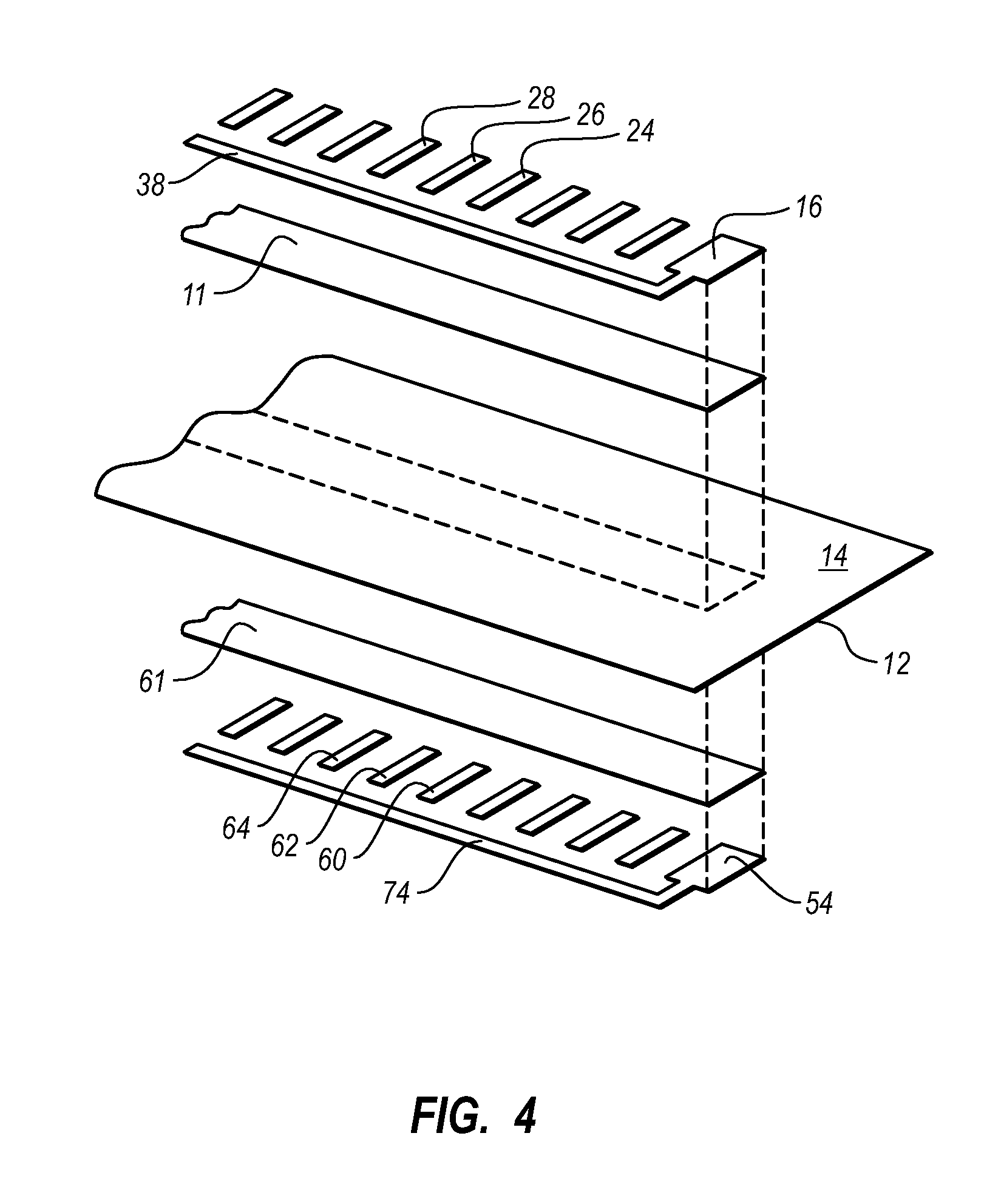
[0031]The bottom surface 50, shown in FIG. 3, is essentially a mirror image of top surface 14 and will be described in greater detail herein with respect to FIG. 3. As such, any explanation of materials, dimensions, etc. that are described with respect to the top surface ...


PUM


Abstract

A system and method for a bi-directional deflectable resistor. The bi-directional deflectable resistor has a first layer of conductive material on a top surface of a substrate and a second layer of conductive material on a bottom surface of a substrate, each layer having a resistance that changes predictably when an electrical signal is applied thereto. The change of resistance of either the first layer of conductive material or the second layer of conductive material reflects an amount of deflection of the respective layer. Having two layers of conductive material allows for the measurement of deflection in all directions.

Description

BACKGROUND OF THE INVENTION[0001]1. The Field of the Invention[0002]This invention relates to electrical components and more particularly to deflectable resistors which vary in electrical resistance.[0003]2. The Relevant Technology[0004]Potentiometers are standard elements of electrical and electronic circuits. They are widely in use today for a variety of purposes including the measurement of mechanical movement. Even though potentiometers are presently available, for example U.S. Pat. No. 5,157,372 (Langford) and U.S. Pat. No. 5,583,476 (Langford), which are incorporated herein for all purposes, no bi-directional deflectable resistor is known to applicant that produces a consistent and predictable variable electrical output upon deflection or bending between configurations occurring in opposite directions from a static configuration.[0005]The use of electrically conductive inks in association with electrical or electronic circuitry is also known. For example, U.S. Pat. No. 4,649,7...

Claims


Application Information

Patent Timeline
Patent Type & Authority Patents(United States)
IPC IPC(8): H01C7/10H01C7/13
CPCH01C10/16H01C10/26H01C10/20
Inventor BECK, DAVID B.SINDT, JOHN A.DANIELSON, THOMAS E.
Owner SENSITRON INC
Learn More